 Animal Location Tracker (A3038)
© 2020-2024 Kevan Hashemi, Open Source Instruments Inc.© 2021 Jordan Kaufman, Open Source Instruments Inc.
© 2022 Nathan Sayer, Open Source Instruments Inc.
| Summer-20 | Fall-20 | Winter-20 | Spring-21 | |
| Summer-21 | Fall-21 | Winter_21 | Spring-22 | |
| Summer-22 | Fall-22 | Winter-22 | Spring-23 | |
| Winter-23 |
[03-MAY-21] The Animal Location Tracker (ALT) is a combined motion sensor and telemetry receiver for our subcutaneous transmitters (SCTs) and implantable stimulators (ISTs). The ALT provides an array of antennas that decode telemetry messages and measure their power. The power measurements allow the tracker to obtain a power centroid location for each individual implanted transmitters. Because each transmitter has its own unique channel number, we have no difficulty distinguishing between the animals in the cage. The power centroid allows us to measure the activity, movement direction, and proximity of animals cohabiting in a cage.

If we combine the ALT with synchronous video, such as recorded by our animal cage cameras (AACs), the ALT allows us to identify animals seen in the video by correlating their movements with the movements of their implanted transmitters.

The A3038A/B/C provides an array of fifteen antennas on a 12-cm grid. The platform is 26 cm × 50 cm and is designed to provide reliable measurement of movement in a cage measuring 22 cm × 46 cm at the base. The ALT receives power and communication through a single Power over Ethernet (PoE) socket at the right side of the platform. To obtain reliable reception and movement measurement, the ALT must operate within a Faraday enclosure, such as our bench-top, stackable FE3A, or our canopy enclosure FE5A. We connect the ALT to an RJ-45 feedthrough in the wall of the enclosure with a shielded CAT-5 cable, and from there to a PoE switch with either a shielded or unshielded CAT-5 cable. We connect our data acquisition computer to the same PoE switch and so record signal and centroid data from the ALT to disk with our LWDAQ Software. Comparing the ALT to the components of our traditional telemetry system, the ALT combines the functions of our LWDAQ Driver (A2071E), Octal Data Receiver (A3027E), and Loop Antennas (A3015C) into one assembly with only one cable.

Our implanted transmitters emit 7-μs bursts of electromagnetic radiation in the range 902-928 MHz. Each burst contains a digital message. Each antenna provides a measurement of radio-frequency power in this same frequency range. When one of the antennas reports that a message transmission is in progress, all fifteen antennas record the power they are receiving. The A3038 saves the transmitted message, along with fifteen eight-bit power values, in its memory, available for download by the Receiver Instrument in the LWDAQ Software, or download and storage to disk by the Neuroplayer Tool. The Neuroplayer contains a Tracker button that opens the Neurotracker Panel, which displays the power centroid of transmitters on the tracker platform.
If we have several ALTs in the same Faraday enclosure, they will receive signals from transmitters on one another's platforms, so the ALT allows us to specify which channels we want it to record. We can specify a list of channels in the Neurorecorder. By default, the ALT records all channels. The activity lamps on the ALT are bright. Once we are satisfied that our recording is proceeding well, we turn off the lights with the HIDE button, so as to avoid disturbing our subject animals. We turn the lights on again with the HIDE button also.
The Animal Location Tracker (A3038) replaces the Animal Location Tracker (A3032). The A3032 provided an array of antennas to track transmitters, but did not itself decode transmitter signals. The A3038 uses each antenna both as power meter and data receiver. We present the basis of the power centroid measurement in our A3032 Feasibility Study and our A3032 Development. The power centroid provides a robust measurement of activity, direction, and proximity of animals. The correlation between the ALT movement and video blob-tracking permits us to be 100% certain which video blob corresponds to which animal, even when there are several near-identical animals in the field of view.
[05-APR-23] The following versions of the Animal Location Tracker (A3038) exist.
| Version | X (cm) | Y (cm) | Coil Pitch (cm) |
Detector Modules |
Base Board |
Antenna Location |
Num Detectors | Comment |
|---|---|---|---|---|---|---|---|---|
| A3038A1 | 51 | 27 | 12 | A3038DM-B | A3038BB-A | Detector Modules | 15 + 0 | Obsolete, Green Mask |
| A3038B1 | 51 | 27 | 12 | A3038DM-C | A3038BB-C | Base Board | 15 + 1 | Discontinued, Black Mask, Unshielded DMs |
| A3038C1 | 51 | 27 | 12 | A3038DM-D1 A3038DM-D2 |
A3038BB-D1 | Base Board | 15 + 1 | Discontinued, Shielded DMs |
| A3038C2 | 51 | 27 | 12 | A3038DM-D3 | A3038BB-D1 | Base Board | 15 + 1 | Active, SF2908E SAW, DMCK modification |
| A3038D1 | 51 | 27 | 12 | A3038DM-D1 A3038DM-D2 |
A3038BB-D1 | Base Board | 15 + 1 | Active, A3038CF-A coaxial filters |
| A3038X | 22 | 18 | 12 | Any | A3038BB-A | Coaxial UMCC | 2 + 0 | Obsolete, Test Stand |
| A3038Y | 22 | 18 | 12 | A3038DM-D3 | A3038BB-A | Coaxial BNC | 2 + 0 | Prototype, Mini Receiver |
The A3038D, shown below, is an A3038C modified for operation in environments with high-power radio-frequency interference outside the 902-928 MHz operating band of our telemetry system. If we have a 1-kW, 1840-MHz mobile phone base station on the roof of our animal laboratory, telemetry reception by an unmodified A3038C will unreliable, even within one of our FE3A Faraday enclosures. Our solution is to equip each detector module on the A3038C with an additional coaxial filter that provides further rejection of out-of-band interference.

We construct the A3038 out of a number of electronic sub-assemblies. Each sub-assembly has its own version number, as we present in the table below.
| Version | X (cm) | Y (cm) | Antennas | Comments |
|---|---|---|---|---|
| A3038DM-X | 18 | 5 | 33-nH Grounded Inductor | Power and signal detector test circuit, A303801X. |
| A3038DM-A | 5 | 3 | 250 nH Grounded Inductor | Detector module, green mask, unshielded, A303801A. |
| A3038DM-B1 | 5 | 3 | 20-mm Ungrounded Helix | Detector module, green mask, unshielded, A303801B. |
| A3038DM-B2 | 5 | 3 | Coaxial Connector | Detector module, green mask, unshielded, A303801B. |
| A3038DM-C1 | 5 | 3 | Coaxial Connector | Detector module, black mask, unshielded, A303801C. |
| A3038DM-C2 | 5 | 3 | Coaxial Connector | As A3038DM-C1, but 2-dB attenuators, SF2098E filter. |
| A3038DM-D1 | 5 | 3 | Coaxial Connector Only | Detector module, black mask, shielded, A303801D. |
| A3038DM-D2 | 5 | 3 | Coaxial Connector Only | As A3038DM-D1, 2-dB attenuators. |
| A3038DM-D3 | 5 | 3 | Coaxial Connector Only | As A3038DM-D2, SF2098E filter. |
| A3038BB-X | 51 | 27 | On Detector Modules | Base board, power only, A303802A. |
| A3038BB-A | 51 | 27 | On Detector Modules | Base board, green mask, A303802B |
| A3038BB-B | 51 | 27 | On Detector Modules | Base board, black mask, A303802C. |
| A3038BB-C | 51 | 27 | Mounted on base board | Base board, black mask, A303802D. |
| A3038BB-D1 | 51 | 27 | Mounted on base board | Base board, black mask, A303802E. |
| A3038BB-D2 | 51 | 27 | None | Base board, black mask, A303802E. |
| A3038CF-A | 2.5 | 1.0 | Coaxial Connector Only | Coaxial filter, SF2098E SAW, 1-dB attenuators. |
[15-JUN-23] The following files provide details of the design and construction of the A3038 base board and detector modules.
S3038X_1: Schematic of prototype power detector and demodulator.If you want to control an A3038 with your own data acquisition software, consult the LWDAQ Spectification for details of the TCPIP messages we use to communicate with the A3038. The A3038 acts like a LWDAQ Driver for the purpose of data acquisition. Its controller address space is defined in VHDL as follows.
constant cont_id_addr : integer := 0; -- Hardware Identifier (Read)
constant cont_sr_addr : integer := 1; -- Status Register (Read)
constant cont_djr_addr : integer := 3; -- Device Job Register (Read/Write)
constant cont_hv_addr : integer := 18; -- Hardware Version (Read)
constant cont_fv_addr : integer := 19; -- Firmware Version (Read)
constant cont_crhi_addr : integer := 32; -- Command Register HI (Write)
constant cont_crlo_addr : integer := 33; -- Command Register LO (Write)
constant cont_cfsw_addr : integer := 40; -- Configuration Switch (Read)
constant cont_srst_addr : integer := 41; -- Software Reset (Write)
constant cont_fifo_av_addr : integer := 61; -- Fifo Blocks Available (Read)
constant cont_fifo_rd_addr : integer := 63; -- Fifo Read Portal (Read)
We memory portal address is 63 (0x3F), as in all LWDAQ controllers. But the A3038's memory portal is read-only. The A3038 does not support the stream_write instruction. It does, however, provide a stream_read, and it is the stream read that we use to download telemetry data from the A3038's controller memory. The telemetry data is stored in a first-in, first-out (FIFO) buffer in the controller. To operate an ALT, the data acquisition software begins by writing any value to the Software Reset location (41), which resets the message clock, clears the message buffer, flashes the white lights, and configures the detector modules. After that, keep reading the Blocks Available location (61). Multiply the blocks available by 512 to get the number of bytes available. The maximum value of this counter is 255, so if there are more than 130 kBytes of data available, you will not know it. The ALT data is divided into twenty-byte message. Each message begins with a four-byte SCT record, which we describe elsewhere. After that come sixteen bytes of power measurements. These are the fifteen detector coil power measurements followed by the power measurement of the auxilliary antenna input. When we download from the ALT, we download a whole number of messages, so the number of bytes should be divisible by twenty. We now execute a stream_read and download the number of bytes we expect.
If you want to configure the ALT to record only from certain SCT channel numbers, you can do this by writing commmands into the controller using the Command Register (two bytes) and the Device Job Register. You will find Tcl code for configuring the ALT in Receiver.tcl.
[23-JUN-21] The front end of the ALT is the one with the twenty indicator lamps. The back end is the one with the Ethernet socket. We place the A3038 in a Faraday enclosures with the front end facing us. We plug a shielded network cable into the ALT's Ethernet socket, and we plug the other end of this cable into an Ethernet feedthrough in the wall of our Faraday enclosure. This interior cable must be shielded to stop Ethernet signals interfering with our subcutaneous transmitter signals. If we are working in bench-top enclosure such as the FE3A, we use an Ethernet feedthrough in the back wall of the enclosure. If we are working in a canopy enclosure such as the FE5A), we use an Eight-Way Ethernet Feedthrough (A3039D) taped to the enclosure floor. Outside the enclosure, we the Ethernet feedthrough to a Power over Ethernet (PoE) switch such as the PoE-16, PoE-8, or PoE-5. For this exterior connection we can use either a shielded or unshielded cable. We prefer to use an unshielded cable outside the Faraday enclosure because unshielded cables are more flexible and they also reduce the chance of ground loops in our electrical system.
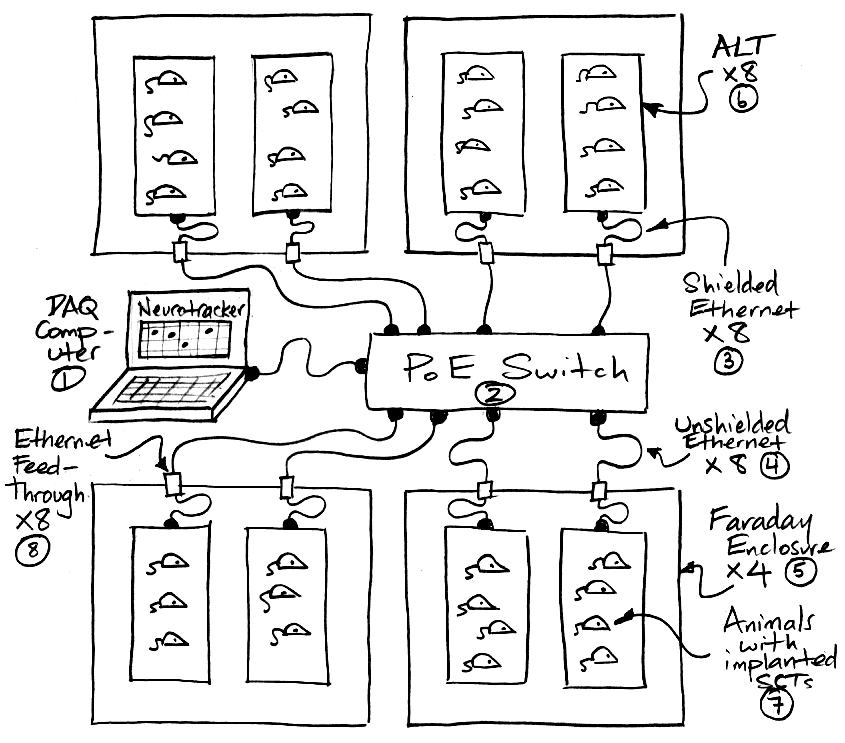
When we complete the connection of the ALT to the PoE switch, the ALT should turn on within a few seconds. The white lamps flash all at once, and then the green lamps turn on and stay on to indicate the presense of 3.3V and 5.0V power. The red button on the front end is the hardware reset button. Press and release the red button and the white lamps will flash again. There are two more buttons on the front end, labelled Show and Hide. Press Show and all the indicator lamps on the ALT will turn on, to confirm that they are working. Press Hide once and all the lamps will turn off, with the exception of the two green power lamps, which will remain on. Press Hide again and the indicator lamps are enabled once more.
We connect our data acquisition computer to the same PoE switch. In the LWDAQ Software we open the Neurorecorder in the Spawn menu. We select A3038A and enter the IP address of our ALT. We ship the ALTs with IP address 10.0.0.x, where "x" is the last three digits of the serial number on the ALT circuit board if less than 255, or the last two digits if greater than 254. Thus P0136 ships with address 10.0.0.136, but C0591 ships with address 10.0.0.91. With the Recorder's PickDir button, choose a directory in which to record the ALT signals. Press Reset. We should see the ALT's white lamps flash. We press Record and the Recorder will begin downloading telemetry signals and antenna powers from the ALT and writing them to an NDF file on disk. We should see the amber Upload light shining to show that the ALT is uploading data to our computer, and the Empty light should flash also, to show that our computer is emptying the ALT's data buffer.
Until we place some transmitters on the ALT platform, we will be recording only clock messages to disk. So we now place some transmitters, or animals with transmitters implanted, on the ALT platform. There are fourteen white lamps to show activity from SCT channels. An SCT with channel number n will illuminate lamp number n modulo 16. So channel 12 illuminates lamp 12, and so does channel 28. There is one blue lamp to indicate metadata channel activity. With the Faraday enclosure sealed, we should see the white activity lamps shining steadily for each of our transmitters.
We open the Neuroplayer in the LWDAQ Spawn manu and select our NDF file for playback. We press Play. If we started with no transmitters on the ALT platform, we will see no signals at first, but the Player will soon catch up with the recording and we will see the live data being recorded from the ALT. Press Tracker to open the Neurotracker. The Neurotracker shows us a map of the ALT platform, with the transmitter locations marked in colored dots. We can export SCT signals, ALT power centroid measurements, and ALT antenna power measurements as text or simple binary files using the Player's Exporter. In both the Tracker and Exporter, we specify the ALT location sample rate in samples per second (SPS). The ALT can, in theory, provide one location measurement per SCT sample it receives. So we could set the ALT sample rate equal to the SCT sample rate. But the ALT does a better job of rejecting collisions and interference if we allow at least eight SCT samples per ALT sample. The default ALT sample rate is 16 SPS.
[15-JUN-23] The A3038 provides an array of antennas. Each antenna is mounted on a detector module. The detector modules are identical. They provide five indicator lamps. The green lamp turns on when the detector module has power and is receiving its clock signal from the base board. The red lamp turns on to indicate an error condition. When the red lamp flashes for half a second, its message buffer has overflowed at least once since the last detector module reset. When the red lamp flashes for one second, its message buffer was empty when the base board controller attempted to read a message from the detector module at least once since the last detector module reset. When the red lamp is on continuously, the detector module's phase-locked loop (PLL) has failed to lock to the base board's 8-MHz clock, which means the detector module's clock is not set to 40 MHz and reception will be impossible. The yellow lamp flashes for 800 μs every time the decoder detects an incomplete incoming message. Whenever one detector module detects an incoming message, auxiliary detector modules measure the incoming microwave power on their antennas. The white lamp flashes for 800 μs whenever a complete message has been received without error. When one detector module receives a message, all detector modules store their power measurements in a buffer. The brightness of the blue lamp increases with the power of received signals. The blue lamp is most useful when only one subcutaneous transmitter (SCT) is moving over the array.
The ALT detector modules are identical circuit boards we plug into sockets on the ALT base board. The detector modules are connected in a daisy chain, where the data from the sixteenth modules moves through all the other modules on its way to the ALT controller. If we unplug the first module in the daisy chain, the controller will be unable to read out any of the remaining fifteen modules. The position of each module in the daisy chain is marked on our A3038C_DMs photograph. If you see red lights flashing, see if you can identify one module that must be blocking the daisy chain readout. If so, follow our ALT_Repair video to remove the ALT cover and re-position the offending detector module.
For each message received from a transmitter, each detector module provides its own eight-bit power measurement. This eight-bit value is a logarithmic measurement of the power received by the detector module from the transmitter when it transmitted the message. The A3038B/C provides an array of fifteen antennas, each connected to a detector module, plus an auxiliary detector module to which we can connect an external Loop Antenna (A3015C) to improve reception or detect background interference. Each message downloaded from the tracker consists of twenty bytes. The first four bytes are the core of the transmitter message, as described in detail elsewhere. The first byte is the channel number. Dual-channel transmitters use two channel numbers to transmit their two signals in separate messages. The second and third bytes are a sixteen-bit sample value. The fourth byte is a time stamp. The ALT messages adds an additional sixteen-byte payload to the core of the message. These sixteen bytes are the sixteen power measurements provided by the detector modules. Their ordering is given by the tracker's geometry drawing. In the case of the A3038B/C, the auxiliary detector power is not shown on the geometry drawing, but it takes the last place in the twenty-byte message.
Our objective is to use the power measurements to obtain a two-dimensional power centroid position that is related to the actual transmitter position in the following ways. The distance moved by the power centroid should be negligible when the distance moved by transmitter is negligible. The distance moved by the power centroid should increase with increasing distance moved by the transmitter. The direction in which the power centroid moves should be strongly correlated with the direction in which the transmitter moves. We the power centroid position is a weighted centroid of the power received from the transmitter in the antenna array, or a weighted centroid of some function of the power. We might use the square root of the power, for example, instead of the power itself.
When we calculate the power centroid position, we start by choosing a sample rate for the calculation. If we choose 8 SPS and our transmitter provides 256 SPS, we expect to have 32 power measurements from each antenna for each of our centroid calculations. We take the median of these, so as to reject corrupted power measurements that arise from transmitter collisions and interference. For each tracker centroid sample, we now have fifteen median eight-bit power measurements, one for each antenna in the array.
The eight-bit power measurements in the ALT message are logarithmic. If the power measurement increases by k, the power has increased by some constant factor g. For the A3038A/B/C, each +33 corresponds to ×10 in power. We could also say that +66 corresponds to ×10 in electric field strength, which is proportional to the square root of the power. We convert the eight-bit power measurements into a value proportional to power with a decade_scale of 33. We convert them into values proportional to the square root of power with a decade_scale of 66. In general, we specify a decade_scale to conver the logarithmic power measurements into a power weight that we will use in our weighted centroid calculation of power centroid. The Neurotracker allows us to set the decade_scale we use for the centroid calculation. We say that power measurement 0 has power weight 1, measurement decade_scale has power weight 10, measurement 2 × decade_scale has power weight 100, and so on.
Once we have the power weights, we multiply each one by the coordinates of its antenna, as given in the geometry diagram, and divide by the sum of the power weights, to obtain the power centroid. We perform the calculation for x and y separately, because they are independent. The result is in the same units as the geometry dimensions. We give ourselves the option of ignoring the power measurements of antennas that are more than extent_radius from the antenna with the maximum power measurement. By default, we se the extent_radius to a value larger than the diagonal of our tracker platform, so we use all antennas. But in the future, if we make a tracker that uses antennas in various places in a maze, the power centroid will be able to tell us where an SCT is in a maze, and the extent_radius would permit us to obtain a robust determination of the animal's progress. We have been using either 33 or 66 for the decade_scale. When we use 66, our power centroid is better-behaved, but contracted towards the center of the platform. When we use 33, our centroid will move to the edges of the platform when the transmitter is above an edge antenna, but the centroid tends to jump at times in a way that does not reflect the actual movement of the transmitter.
[13-JAN-22] The A3038 draws its power from its Power over Ethernet (PoE) socket, J16, on the right side of the board. An DC-DC converter, L1, produces 5.0 V from the PoE's 48 V. Another converter, U1, produces 3.3 V from 5 V for use by the RCM6700 single-board computer. We measure the power consumption of the A3038 by connecting 5 V directly to the 5-V supply rail, thus by-passing the DC-DC converter, and measuring the current drawing from the 5 V supply. We then assume 80% efficiency in the converter to obtain an estimate of power consumption. By this means, the A3038C consumes 7.8 W.
[25-OCT-22] Quality control consists of five stages: QC0-QC4. We gather detector modules into sets of sixteen, and eventually install them on a single base board. Each detector module receives a serial number consisting of four hex digits, which we adhere to the logic chip. We program and calibrate ALT Detector Modules (A3028DM) with a fragment of a prototype base board, shown here. Once programmed, we measure current consumption and record in our Quality Control Zero table. Typical current consumption for A3038DM-3 detector modules is 67-69 mA. We mow move the detector module to a Test Stand (A3038X), where it receives power and a clock signal so that it can receive messages.

We drive the VCO with a 10-kHz 2-Vpp positive ramp, and trigger on the negative edge at the end of the ramp. We a −40 dBm sweep produced by the VCO and attenuators to A and look at P. We should see something like the trace below.

We should see the SAW filter pass band 900-930 MHz on P. We set up cursors to mark the two extremes of the pass band. Now we apply the sweep to B with UMC socket P2 and look at the demodulator output, D. We want the peak response of the tuner to be in the range 930-940 MHz, with 930 MHz being ideal. The ideal response is shown below.

We adjust the peak frequency with trimmer capacitor C15, which we can turn with a small flat-head screwdriver. In earlier versions of the DM, we hand-loaded capacitors until we had the tuning correct. From these calibrations, we have examples of final component values and peak frequencies, see here. Once the tuner is calibrated, we add another 10-dB attenautor to our sweep and apply the −50 dBm sweep to A with P1. We examine D and should see some adequate response like the one shown below.

Following calibration, we turn on our −8 dBm SCT signal generator and keep adding attenuators until the detector module's white reception light starts to flicker, indicating the signal is becoming too week for reliable reception. We record the SCT signal power as the sensitivity of the detector module. Typical sensitivity for A3038DM-D3 are −59 down to −63 dBm. We record the sensitivity to complete Quality Control Zero.
The detector module now moves to Quality Control One, where we apply a −70 dBm sweep to A and observe power at C. We plot and print the sweep response for all sixteen detector modules in one plot, as shown below.

Quality Control One continues with application of −80 dBm, −60 dBm, −40 dBm, and −20 dBm to A at 915 MHz while we record by hand the power we observe at C. The output C of the limiting amplifier should be constant to ±0.5 dB from −60 dBm to −20 dBm. At −80 dBm we see erratic behavior as interference dominates the limiting amplifier, whereupon our 915 MHz output power will drop, or fails to dominate, whereupon our 915 MHz output power will rise again to its maximum value. Saturation power levels with a 50-Ω spectrometer added to point C are −14.5 to −16.0 dBm. This amplitude response table completes Quality Control One.
Quality Control Two consists of setting up a base board, programming its firmware, configuring its Ethernet interface, and loading the detector modules. We record from the ALT to disk. We check for correct functioning of the base board, looking for red error lights on the detector modules. Before connecting the antennas or loading the shield covers, we measure background and minimum reception power. For background, we record the powers from channel zero, which is the ALT background power measurement. For sensitivity, we hold a transmitter near the input of each detector module and watch for 95% reception in the Neuroplayer. We have the Neuroplayer showing us the power from each detector module, and so we record the minimum power measurement in units of ADC counts for which each detector module obtains 95% reception.

We connect antennas and load shield covers on the detector modules from DM1 to DM16. We place our transmitter directly over the detector coil and record maximum signal power. We check tracking by moving around the perimeter and by hovering over each coil. We place in a Faraday enclosure and measure interference power now that our coils are connected. The result is the table above.
In Quality Control Three we place the ALT in a Faraday canopy and swing a transmitter over its full length on a damped pendulum. We record the motion using the ALT and confirm that the period we observe is correct and steady, and that the amplitude decreases as does the damped motion of the pendulum.

In Quality Control Four, we place the ALT in a Faraday enclosure with several transmitters and record continuously for forty-eight hours, looking for errors in communication and red lights on the detector modules. If recording is sustained and flawless, and there are no red lights on the detector modules, the ALT is ready to ship.
[16-SEP-20] The A3038DM-X requires the addition of four 10 nF and four 47 pF decoupling capacitors for U1-U4, as well as two 100 pF capacitors around U6.
[25-JUL-21] The A303801B printed circuit board needs the following corrections for A303801C. The schematic for the updated detector module is S3038D_1 and S3038D_2
[07-JUL-21] We make the following modifications to the A303802B PCB when preparing the A303802C.
[07-MAY-21] The A3038BB-A requires the following modifications when built with the A303802B.
[29-JUL-21] The A3038DM-C made with the A303801C requires the following circuit board modifications.
[27-JUL-21] The A303801C requires the following modifications when preparing the A303801D. Use the A3038D schematic for netlist check.
[29-AUG-21] The A303802D requires the following modifications when preparing the A303802E.
[21-NOV-21] The A302802E requires the following modifications when preparing the A303802F.
[26-OCT-22] The Detector Module Clock Modification, whereby we load DC7, which is the 8-MHz DMCK, with 100 pF close to its source on the base board, so as to reduce edge reflections from the far end of the detector module bus.

We introduce this modification for the A3038BB-D1 and A3038BB-D2 base boards constructed with the A303801E printed circuit board. These base boards are used in the A3038C2 and TCB-A16 respectively.
[14-JUL-20] We examine the response of the A3032C ALT amplifier and detector. We apply a −6 dBm sweep 840-980 MHz to a Loop Antenna (A3015C). We generate the sweep with a Modulating Transmitter (A3014MT), and we split the sweep and mix with 910 MHz to produce an IF ±70 MHz, which we run through a 21-MHz low-pass filter before viewing on the scope. We hold the loop antenna above Coil 10 on V0384 and observer the following response on PW, which is U1004-3.

We repeat on all fifteen antennas and find the same response on each one, ±100 mV variation in 890-930 MHz, which is roughly ±3 dB. We remove the A3051C loop antenna and replace it with a 3-dB attenuator and a 50-mm bent wire antenna. We observe the same ±3 dB variation on power through the pass band. But in rare orientations of the antenna, all surrounding objects remaining stationary, received power drops suddenly, and variation is ±6 dB.
[29-JUL-20] We are considering using detector diode such as the SMS7630 in our antenna amplifier to provide power limiting and power detection.

In SkyWorks application note APN1014, we see the detector circuit they used to obtain the above rectified voltage versus input power. They deliver power from a 50-Ω source, but do not load the source with 50 Ω. Instead, they place a diode and balast capacitor in series with the 50-Ω source impedance. The voltage across the diode will be roughly double what we would see if we loaded the source with 50 Ω. Their "Incident Power (dBm)" is the power that reflects off the detector circuit, which would be equal to the power delivered to a 50 Ω load. The "video resistance" they refer to in the detector plot is the resistor loading the balast capacitor.
We assemble a power detector made out of an SMS7630 diode and a 100 pF balast capacitor attached to a 50-Ω transmission line carrying the output of an A3029B amplifier. We measure the voltage across the balast capacitor, which we call the rectified voltage. We vary the transmission line power from −30 dBm to +28 dBm. Below −30 dBm our rectified voltage is swamped by noise. At +28 dBm, our amplifier is saturating. When we remove the diode and capacitor, our amplifier saturates at +30 dBm. With +6 dBm we add 1 kΩ in series with the diode and see only 90 mV, compared to 360 mV with no resistor.

We solder 51 Ω from the center pin of a BNC socket to ground. In parallel we place a SMS7630 diode and a 1.0 nF balast capacitor. We supply power down a 1-m coaxial cable from our synthesizer, and vary power from −30 dBm to +10 dBm. We measure the voltage rectified voltage versus power and plot.
[30-JUL-20] We solder a 33 kΩ resistor across a BNC socket. In parallel we place a SMS7630 diode and a 1.0 nF balast capacitor. We connect the detector directly to the output of our synthesizer. Without the 33 kΩ, we see no sustained rectified voltage, because the incoming power is capacitively coupled.
[07-AUG-20] We have the schematic of a prototype detector module, which provides both power measurement and demodulation of SCT messages, S3038X_1. Top view of circuit board here. This circuit will provide the D input for an A3007D so as to provide SCT signal reception, and will also produce an output P from the power meter. Power supply will come from a two-pin molex plug.
[04-SEP-20] We assemble a prototype detector module (A3038DM-X), as in S3038X, except we omit U5. We remove L1 so that we can supply A through J1. We remove R9 so that we extract B through J2. We connect 3.0V to P1. We see 33 mA flowing in. With four of BGA2803 and one of LT5534 we expect 31 mA. We connect J2 to our hand-held spectrum analyzer, and J1 to our frequency synthesizer, with attenuators as needed, to obtain the following plot of B versus A for 910 MHz.

The BGA2803 gain at 910 MHz is 24 dB. We have three 3-dB attenuators for −9 dB. We have the insertion loss of the SAQ filter L2, a B3588, which is around 2 dB. We expect the gain of the first two stages to be 37 dB. We see 41 dB from −90 to −50 dBm input. The output of U2 saturates at −5 dBm, which is consistent with the BG2803 data sheet.
We remove R1. Now we are shorting the input to ground with R17. We see 0.5 V at the output of the power detector, P, indicating −49 dBm at the input of the power detector, which implies −90 dBm at the input of U1, which is consistent with 50-Ω thermal noise in 900-930 MHz. When we restore R1, with our frequency synthesizer still attached, we see 1.8 V on P, meaning B is −17 dBm, which suggests interference of −58 dBm.

We apply −60 dBm to A and measure B as we vary frequency. We see the pass-band of the SAW filter clearly. We are surprised by the higher gain at 900 MHz and 930 MHz, which mark the edges of the pass-band. We restore R2 and sweep frequency again, this time measuring power at J4.

Output J4 is flat to within ±1 dB in the SAW filter pass band, at around −6 dBm. Diode arrays DA1 and DA2 are SMS7630. Their saturation current is 5 μA, so we expect their dynamic resistance to be 50 Ω for forward voltage 110 mV. Our guess was they would limit the amplitude to −3 dBm. But B and J4 are limited to −5 dBm by the BGA2803 saturation alone. We predict that removing DA1 and DA2 will change nothing. We would like B to lie in the range −60 dBm to 0 dBm when detecting transmitter power bursts. But we can receive up to −20 dBm from a transmitter held close to an antenna. The gain from A to B is 21 dB too high.
[07-SEP-20] We apply −52 dBm 910 MHz to A. We have L1 and R9 removed. We measure −10 dBm at B. Gain is 42 dBm. We mix with +7dBm of 880 MHz using a ZAD-11 and see IF amplitude is 50 mVrms, or −13 dBm (conversion loss only −5 dBm). We sweep the frequency from 820-980 MHz and obtain the following IF trace.

Gain in this measurement is constant to ±2 dB in the pass-band of the SAW filter. We do not see the +10 dB ears that appear in our measurement using our hand-held spectrometer. For −10 dBm we expect 2.2 V at P. We see 2.4 V. We vary power supply voltage and measure gain and supply current.

We restore R9 and apply −36 dB sweep 820-980 MHz to A. We mix the same sweep with 910 MHz to produce IF that we pass through 21 MHz low-pass filter. We have L3 = 3.3 nH, C16 = 0.5 pF, C17 = 2.0 pF, C18 = 10 pF, R25 omitted. We have U5 loaded and feedback configured for D = 4R. We look see the following tuning curve on D.

We see D go from 0.5 V at 894 MHz to 2.5 V at 936 MHz, which is perfect for demodulating SCT signals. We apply an SCT signal −31 dB, to A. With no R25 and C18 = 10 pF, our SCT demodulated signal is a triangle wave. The rise time of D appears to be around 200 ns. Add R25 = 1 kΩ and see the trace below, rise time around 50 ns.

The above signal is similar to the traces we see in our downshifting receivers. We repeat our frequency sweep to see again the tuning response. We now have D going from 0.2 to 0.9 V in the band 894-936 MHz.

We try C18 = 0 pF with R25 omitted. We see the same demodulation sweep amplitude as for C18 = 10 pF with R25 omitted, but when we apply an SCT signal, the rise time is around 100 ns.
[10-SEP-20] We remove R1. We connect C13 to R6/R7 instead of B. We see 0.74 V on P. We load 100 pF from U6-4 to 0V and see 0.40 V. Adding another 100 pF makes no difference, nor does adding 10 pF. We load 100 pF across P1 and see 0.35 V on P. As soon as we restore R1, even without L1, we see 1.1 V. If we connect 50 Ω to J1 we see 0.44 V. With L1 loaded and J1 open circuit 1.1 V. Restore C13 to its previous connection and see 2.1 V on P. Remove R1 and see 1.2 V.
[12-SEP-20] Restore R1 and see 2.1 V on P. We test the hypothesis that J1 and L1 are picking up radio waves transmitted by J4, and the 80-dB total gain of the amplifier is generating oscillations at a frequency above 2.4 GHz. We rotate C7 and C10 so that they connect U3-6 and U4-6 to 0V. We still see 2.1 V on P. We rotate C4 to connect U2-6 to 0V. We connect C13 to R7, so we have U2, U3, U4 with grounded inputs, their outputs loaded by attenuators, and U6-6 driven by R7. With L1 loaded and J1 open circuit, P = 1.1 V. Remove L1, P = 1.1 V. J1 is not picking up radio waves from J4.
[14-SEP-20] We restore R1, restore C13 to B, and restore C4. Now we have amplifiers U1 and U2 working, driving R9/R10 attenuator, and also driving our spectrometer through J2. Amplifiers U3 and U4 have their inputs grounded with capacitors. The A3038X and spectrometer are inside a Faraday enclosure, and we have a 10-dB attenuator between J2 and the spectrometer. We see P = 2.1 V and B has peaks 1053 MHz −10 dBm, 886 MHz −50 dBm, and 929 MHz −55 dBm. We replace L2 with a wire link. We see P = 1.9 V. The spectrum of B contains peaks 1226 MHz −11 dBm, 1297 MHz −22 dBm and several others. Remove R1 and see P = 1.6 V and B has peaks 1220 MHz −21 dBm, 1261 MHz −26 dBm. Restore L2 and remove J1. See P = 2.1 V and B has peak 1061 MHz −4 dBm. Remove U1 and replace with wire link, P = 0.8 V, B has peak 1217 MHz −42 dBm. Replace L1, P = 2.1 V, B has peak 1037 MHz −7 dBm. Load 27 Ω for R1, R2, and R17. Now P = 0.8 V, B has peak 1221 MHz −42 dBm. Connect test transmitter, transmit off, peak 929 MHz −44 dBm. Turn on −38 dBm transmit signal and see P rising to 2.2 V. We load R1 = R2 = 15 Ω and R17 = 75 Ω. With J1 open circuit, B has peak 1010 MHz −10 dBm. With J1 connected to 50-Ω coax peak is 929 MHz −52 dBm and B is 0.8 V. With L1 loaded and J1 open, P = 1.8 V and B has peak 961 MHz −17 dBm. We load UPC2746T in place of U1, and restore R1, R2, and R17. With J1 open and L1 loaded, B has peak 840 MHz −12 dBm. Connect J1 and peak vanishes. Restore BGA2803 for U1 and load 0 Ω for R1/R2 and 50 Ω for R17. On P 2.1 V, on B 1012 MHz −8 dBm. Remove R1 and see P = 0.9 V. Remove R2, P = 0.9 V. Load R1 = R2 = R17 = 51 Ω. Have P = 1.0 V, B peak 929 MHz −46 dBm. Connect −68 dBm SCT signal and see P rise to 1.2 V during burst.
With L1 and J1 loaded, and R1 = R2 = R17 = 51 Ω, apply −8 dBm SCT signal to A3015C loop antenna. A3038X in Faraday enclosure. Can see signal clearly on B at range 50 cm. Take A3038X out of enclosure and hook up to P and D as well as trigger from SCT. Apply −48 dBm SCT to J1. See SCT signal clearly on DA, and P rises from interference level 1.5 V to burst level of 2.0 V. Disconnect SCT and connect spectrometer to B, see −27 dBm in 902-928 MHz, with P varying 1.0-1.5 V. Connect −8 dBm SCT signal to A3015C. Reception range outside Faraday enclosure is only 10 cm.
[16-SEP-20] We restore R1 = R2 = 8.2 Ω and R17 = 150 Ω. We remove L1. We see P = 2.22 V as the circuit oscillates. We have 47 pF capacitors in P0603 package (Digikey 445-1277-1) with self-resonant frequency 900 MHz. We connect directly from pin U1-2 to C3-2 to add local decoupling. Now P = 1.24 V. We add 47 pF to U2 in the same way, P = 1.16 V. We load a second 47 pF in parallel to the one next to U1 and P increases to 1.64 V. So we remove that capacitor and add one to U3 and U4, so each has its own local 47 pF. Now P = 1.10 V. Again we double-up 47 pF next to U1, again P increases to 1.64 V. We move the two 47 pF and mount them on C3, P = 2.02 V. Remove one 47 pF, leaving one 47 pF on C3, P = 2.08 V. Replace C3 = 100 pF and the 47 pF addition with a single 47 pF, P = 2.04 V. Restore 47 pF next to U1, and load 47 pF for C3, see P = 1.84 V, which turns out to be −21 dBm of 1200 MHz. Replace C3 with 1.0 nF, P = 1.16 V. We remove R1 and P = 1.02 V. We replace C3, C5, C8, and C11 with 1.0 nF and each of U1-U4 has 47 pF soldered to pin two. We see P = 1.04 V. Now we double up the 47 pF on U1, and still see P = 1.04 V. So we remove the two 47 pF and stil see P = 1.04 V. Remove all 47 pF and P = 1.12 V. We restore the 47 pF and see 1.04 V again.
We have R1 = R2 = 8.2 Ω and R17 = 150 Ω, no L1, and combined 47 pF and 1.0 nF decoupling capacitors. We connect −60 dBm of 910 MHz through a 1-m cable to J1 and see −20 dBm at J2, suggesting gain at least 40 dB. At J3 we see +0 dBm and at J4 +2 dBm. Apply −40 dBm input and see +0 dBm at J3 and +1 dBm at J4. Outputs J3 and J4 are after −3 dB attenuators, and we are adding an additional 50-Ω load when we make our measurement, so saturated output power of U3 and U4 appear to be +3 dBm and +4 dBm. According to the BGA2803 data sheet, saturated output power should be −3 dBm. We apply SCT signal to J1 and find we need at least −38 dBm to get demodulated signal at D, even in Faraday enclosure, even when waiting for interference to subside.
[17-SEP-20] We go back to decoupling with 100 pF on their footprints and restore R1 = R2 = R17 = 51 Ω. We apply −58 dBm SCT signal to J1 and see clear demodulated levels on D. We apply −60 dBm from our synthesizer and measure power at B, J3, and J4 by plugging our spectrometer into J2, J3, and J4. We do not remove any resistors. When we plug our cable into J2, J3, or J4, the signal at the connector is loaded by two 50-Ω impedances in parallel. We measure power at each frequency by finding the peak in our spectrometer and observe the following ±5 dB variation in gain in the SAW filter pass-band. (NOTE: On 24-SEP-20 we obtain ±2 dBm gain uniformity within the SAW passband after exchanging L2.)

[18-SEP-20] We have R1 = R2 = R17 = 51 Ω, and no L1. Now we load in parallel with the C3, C5, C8, and C11 10 nF and 47 pF, with the 47 pF right next to the amplifier pins. We have no L1. With J1 open-circuit, P = 0.58 V. We detect −58 dBm SCT clearly on D when 929 MHz interference we pick up with spectrometer antenna is −60 dBm. With −47 dBm interference, D is contaminated with what looks like 50 MHz noise. We apply −47 dBm sweep to J1 and observe D and P.

When we drop the sweep to −56 dBm, we must wait until 929 MHz interference dies down to −69 dBm before taking our photograph.

We load L1 and place A3038X in Faraday enclosure. We look at D while moving a transmitter from one place to another. With the door closed, we see the transmit burst in all locations, and the data bits are clear for ranges up to 10 cm. When the transmitter is farther away, the bits are overwhelmed by 50 MHz noise. We note that the A3027E's superhet receiver provides a total gain of 100 dB with limiting at 6 dBm (±0.7 V) before demodulation, while this amplifier provides 80 dB gain before limiting at −5 dBm at J4.
[21-SEP-20] We have R1 = R2 = R17 = 51 Ω, L1 loaded, apply −40 dBm of 915 MHz to J1. See P = 2.12 V. Load 0.5 pF parallel with L1, see 2.12 V. Load 1.0 pF see 1.40 V, load 1.5 pF see 1.32 V. Remove parallel capacitance.
We have R1 = R2 = 8.2 Ω, R17 = 150 Ω, L1 loaded. Apply −40 dBm 915 MHz, P = 2.36 V (−5 dBm). Apply −50 dB=m, see 2.12 V (−13 dBm). We remove L1. We remove R20, R21, DA1, and DA2. We replace R9, R10, R12, R13 with 0 Ω. We apply − 60 dBm of 915 MHz and see −5 dBm on J4. We remove R19 and replace R6 and R7 with 0 Ω. Apply −50 dBm to J1 and see P = 2.16 V (−12 dBm). Restore R19, R6, R7 and see P = 2.08 V. Removing our 3-dB attenuator between L2 and U2 gives us a 2-dB increase in gain. Of our six attenuators, we leave the first three in place to stabilize the antenna and filter. We remove the fourth and fifth to increase the overall gain. We leave the sixth one in place because it makes no difference to the relative power of any signal, and offers better isolation of the switched capacitor filter. We apply −58 dBm SCT signal to J1 with L1 loaded. When interference dies down we have a clear 200 mVpp SCT signal on D = 4R. With −64 dBm we never get a clear signal.
[23-SEP-20] We measure the reflection coefficient of J1 with L1 loaded and R1 = R2 = 8.2 Ω, R17 = 150 Ω. We apply −20 dBm to the OUT terminal of a ZFDC-10-5+ directional coupler. We connect CPL to our spectrometer 50-Ω input. We connect IN to a 1-m coaxial cable. With 50-Ω termination we see −52 dBm at CPL, suggesting reflection of no more than −41 dBm, or 1% of incident power. We remove terminator and see −29 dBm, suggesting −18 dBm reflected. We call that 100%. now connect to J1 and see −48 dBm on CPL, suggesting −37 dBm reflected power, or roughly 2% reflection.
We remove L2, the SAW filter, so we can see the response of the demodulation tuner. We apply a −26 dBm sweep.

We adjust C16 and C17. We have L3 = 3.3 nH. We measure the frequency and height of the peak in D

We restore C16 = 0.5 pF, C17 = 2.0 pF and restore L2, the SAW filter. We apply a −26 dBm sweep.

[24-SEP-20] We apply 4.5 V power supply to our A3038X by mistake for twenty seconds, but the board seems fine afterwards. Current consumption 33 mA at 3.0 V supply. We replace L2, the SAW filter. We remove L1. We use J2 to bring B to a ZAD-11 RF input, and mix with 820 MHz LO. We choose our LO frequency so it is well outside the pass-band of the SAW filter. We obtain a clean sweep on D for 1000 MHz LO as well. We view the IF on the scope, as well as D and P.

We load L1 and connect a −3 dBm sweep to an A3015C loop antenna. We place the antenna 20 cm from L1. We wait for interference to die down and take the following picture.

We remove L1 and apply −48 dBm SCT signal to J1. When interference subsides, we get clear SCT logic levels on D.
[23-DEC-20] We have A303801A boards for the A3038DM-A RF Detector assembly, schematic S3038A_1 and S3038A_2. We assemble first amplifier stage with R1, R2, R3, and L2. We generate 910 MHz with our synthesizer, carry it through 1.5 m of cable to P1 (antenna input A) and then extract the output from P2 (filtered output B). We do not load the antenna inductor, L1. We have no other load downstream of P2. We forget to include the 10-nF and 10-μF decoupling capacitors on the 3.3-V power supply, but the amplifier performs as below. Current consumption is 6.7 mA.

We add the decoupling capacitors C5, C6, C7, C22, C23, C24, C25. We set the synthesizer to −20 dBm and vary frequency, then repeat with −30 dBm.

In the pass-band of L2 B3588 with −20 dBm input, we see −10 dBm output at B. Assuming 1 dB loss in delivery cables and connectors, 3 dB insertion loss for L2, and 3 dB attenuation in each of R1, R2, and R3, gain in U1 BGA2803 is +24 dB, as specified by the data sheet.
[24-DEC-20] We connect an A3014MT −3 dB output to A through 20-dB attenuator and 1.5-m cable. We measure −17 dBm at B, 916 MHz. We add U2 LT5534 and C31. Current consumption 14 mA. We terminate B with 50 Ω. We sweep A from 850-950 MHz and look at P.


The detector output ranges from 0.2 V to 2.2 V. According to the data sheet, this corresponds to −60 dBm to −5 dBm. We touch the amplifier circuit and the response at P remains the same, except for an overall drop of about 0.2 V when we enclose the entire signal chain in our hand. We load U5, U6, U7 BGA2803 with coupling capacitors. Current consumption is now 36 mA with no input, 39 mA with −10 dBm on input. We have no R5, and connect hand-held spectrometer to P3 (C) via 10-dB attenuator. We apply power to A with synthesizer through attenuators as needed and 1.5-m cable. We measure power at C versus power at A and add to plot above. Power at C increases by 20 dB as we increase A from −70 dBm to −60 dB, which suggests domination of our input by interference.
We load R5, a solder lump for C14, detector diode D1 SMS7630, and 100 pF for C16. Schematic has D1-1 and D1-2 swapped around, we rotate D1. We take the signal from P5 (C) to a ZAD-11 mixer through −10 dB, mix with 915 MHz, and display on scope along with P and R. For A we have a −33 dBm sweep.

The IF is 30 mVpp or −17 dBm. Loss in the ZAD-11 mixer is 7 dB, so C is 0 dBm. We are sharing C between P3 and R5, so C without extraction at P3 would be around 3 dBm, consistent with our plot above. At the output of R5 we should have −3 dBm. Our calibration of the SMS7360 leads us to expect a 100-mV rectified voltage R. We see 20 mV, and outside the pass-band of L2 we see 60 mV. We rotate the diode, switch the diode, change capacitors, isolate the diode output, and no matter what we do, the output is never what we expect. The diode itself has marking XD8, which is correct for SMS7630-006LF.
[26-DEC-20] We build a power detector out of a 50-Ω resistor, 100-pF capacitor, and SMS7630 diode, soldered to the end of a short coaxial cable that we can plug into P2 or P3. We apply −33 dBm 915 MHz to P1. We get 100 mV on our detector when plugged into P3 with R5 removed. Our spectrometer says −1.5 dBm of 915 MHz. If we disconnect the 915 MHz input, we get 200 mV at our detector, implying +1.5 dBm wide-band power at C. If we apply a sweep, we see a 100 mV in the pass-pand of L2, but 200 mV outside the passband. With no input on A, we scan the power at P3 (C) from 250-6100 MHz and see a dozen peaks as high as −29 dBm, but nothing higher. The power at C is greater if we are amplifying interference than if we are amplifying a carrier frequency.
We build the tuner with R5 = −3 dB, C14 = 0.5 pF, C15 = 3.2 pF, L3 = 3.3 nH. We have D1 oriented correctly. We load 100 pF for C16 and omit R6. We apply our −33 dBm sweep again and look at R and P.

The peak of the tuner response is at around 945 MHz, where the attenuation by the SAW filter (L2) is around 30 dB. The −33 dBm sweep at 945 MHz produces −60 dBm at B. The gain of U5-U7 we expect to be around 72 dB, so the output of U7 (C) will still be saturated at 945 MHz.
[28-DEC-20] We load C16 = 10 pF, R6 = 1 kΩ and complete the circuit shown on S3038A_1, ending with the production of logic signal Q at U9-6. Current consumption is 40 mA for 3.3-V power supply. We try various combinations of capacitors and inductors in the tuner, settling upon C14 = 1.0 pF made out of two 0.5 pF in parallel, C15 = 3.2 pF made out of 2.2 pF with two 0.5 pF in parallel, L3 = 3.3 nH. We connect a −58 dBm sweep to P1 (A) and look at P, R, and the RF input mixed with 915 MHz.

We apply −34 dBm SCT signal to A and look at P, R, and F, this last being the output of the demodulation band-pass filter. We load 1.0 kΩ for R6, but we drop C16 to 2.2 pF from our original 10 pF as this improves the fall time of R.

We compare the SCT bit sequence to our receiver output, Q, which is supposed to be the recovered SCT bit sequence for our −34 dBm SCT input.

The received signal is always the same as the original. We drop the SCT power to −44 dBm and the received signal is the same 90% of the time, but we are seeing interference corrupting reception. We are operating out in the open on our bench.
[31-DEC-20] Load remaining components onto A3038DM-A and program U10 with prototype message detector P3038A_Main. We do not put U10 into standby mode. Current consumption of entire board is 47 mA.
[01-JAN-21] We assign LED4 (white) as a message receive indicator and LED5 (blue) as a message ready indicator. The former illuminates when we are receiving a message, but the message has not yet been decoded and accepted. The latter illuminates only when the message has been accepted. We use LED1 for power and we flash LED2 and LED3 to show clock function. Our message decoder is a VHDL translation of the original ABEL decoder P302702A12_Decoder used in the Octal Data Receiver. We connect test transmitter −44 dBm signal to A with P1 and get 100% reception. We remove P1 and load L1. We get 100% reception from an A3028E at ranges 0-2 cm, and some reception at ranges up to 10 cm. In a Faraday enclosure, we have robust reception up to 4 cm from L1, but no farther. Current consumption is 52 mA.
[04-JAN-20] We note that power measured at P is 10 dB lower than we expect. We replace L2, the SAW, and power returns to our previously-measured values. We replace C16 with 10 pF and reception of SCT signal improves. We attach a 3.3-V regulator to a lipo battery and supply the board with clean power. We see a reduction of noise on D. We connect −48 dBm SCT signal to A and obtain intermittent reception. We connect an A3015C loop antenna to A and place in Faraday enclosure with an A3028E. We obtain robust reception at ranges up to 10 cm. We load a 230-nH inductor antenna for L1 and obtain no reception. We are fiddling around and replace U1 and L2 again, but cannot obtain reception from −38 dBm SCT signal. We have 10-MHz noise on D.
[05-JAN-21] We reflow capacitor solder joints, replace connector P1, and clean. We examine the response to an SCT sweep and note roughly 10-MHz ripple in the step-response of D. We place 10-nF capacitors in parallel with decoupling capacitors C3, C8, C9, and C10. The ripple in D persists. We connect our A3014MT modulating transmitter to A through −20 dB and drive it with a 200-mVpp 1-MHz square wave to view the step response of the tuner and detector circuit. We look at D, which is R amplified by five. The signal applied to A is −24 dB of 900-920 MHz.

[06-JAN-21] We remove 10 nF capacitors in parallel with C3, C8, C9, and C10. We remove the tuner and connect R5 directly to D1. We apply RF to A with our synthesizer and find oscillations in D of several Megahertz for constant frequency and power applied to A. As we vary the input power and frequency, the amplitude and frequency of the oscillations varies. We replace C1, C2, C32, C11, C12, and C13 with 10 pF. Previously, when loaded with 100 pF, the corner-frequency of the high-pass filter made by the coupling capacitor and the 50-Ω input impedance of the next amplifier stage, was 32 MHz. Now the corner frequency is 320 MHz. The oscillations of several Megahertz decrease in amplitude by a factor of two.

We apply a −54 dBm sweep and find D to be cleaner than before. Note that we are powering the circuit with the LiPo battery and regulator.

We apply a −24 dBm sweep and observe oscillations on the demodulator output are reduced by a factor of two. We still see the spikes at around 400 kHz, but they are smaller. Note that these spikes exist despite our using a LiPo battery as a power supply, so they are not caused by our bench-top power.

We connect an A3015C loop antenna to A through P1. We place in Faraday enclosure with an A3028E. We obtain reception from 90% of locations within the enclosure, at ranges up to 60 cm across the diagonal. Reception at less than 10 cm is robust.
[07-JAN-21] We apply −60 to −10 dBm 927 MHz to antenna input A with our synthesizer and watch demodulator output D. We see oscillations of 7.5 MHz on D and amplitude 40 mV from −50 to −10 dBm. At lower power, D becomes more chaotic, but we still see the oscillation buried in the noise. We vary the frequency and keep power at −30 dBm.

The oscillation is consistent with an intermediate frequency (IF) created by mixing the amplified synthesizer frequency at C with a fixed interference frequency of 920 MHz picked up by the split-capacitor tuner C14-C15-L3. The amplified synthesizer frequency on C acts as the local oscillator (LO) for mixing at the detector diode D1, and the 920 MHz interference acts as the radio-frequency (RF) input to the mixer. Diode D1's non-linear response to the sum of the LO and RF creates the IF at R. We note that we have a 40-MHz 3.3-V oscillator, U11, on the board, and it's 23rd harmonic will be exactly 920 MHz with amplitude 170 mVpp. This oscillator is mounted directly below the detector diode D1, on the other side of the ground and power planes. So long as the signal applied to A is −60 dBm or higher, we will have LO of 0 dBm, generating roughly the same amplitude RF. The IF amplitude is roughly constant, while its frequency is exactly equal to the difference between the synthesizer frequency and the 23rd harmonic of the oscillator. The 920 MHz RF signal is amplified by the split-capacitor tuner as shown above. When the LO is 915 MHz, right in the middle of our 902-928 MHz ISM band, the IF is 5 MHz, which is the bit rate used by our subcutaneous transmitters (SCTs). The IF passes through the discriminator (C17-19, R9-10) before arriving at the comparator as F. The frequency response of the discriminator is the A3007D trace in this plot. We have maximum discriminator gain at 5 MHz. The 920 MHz interference is optimal for disrupting SCT message reception.
We will try removing U11 to see if the oscillations disappear. We can try 80 MHz for U11, for which the 11th harmonic is 880 MHz. Its amplitude will be roughly double that of the 23rd harmonic of 40 MHz, but the gain of the tuner at 880 MHz is only a quarter of the gain at 920 MHz, as shown above. The IF frequency for 915 MHz mixed with 880 MHz will be 35 MHz, for which the gain of the discriminator is a third of its gain at 5 MHz. So the oscillation for LO of 915 MHz will be 2 × 0.25 × 0.33 = 0.17 the amplitude we see now, or six times smaller.
[08-JAN-21] We remove U11 and the oscillations disappear. We load a new U11 and the oscillations are back, same amplitude and frequency as before. We add 100 pF in parallel with C25, no change in amplitude. Remove both capacitors, no change. Restore 10 nF for C25, same as ever. We order 80-MHz oscillators.
[11-JAN-20] In Faraday enclosure, with 250 nH inductor for L1, battery power, we obtain robust reception at up to 5 cm from an SCT.
[12-JAN-20] We replace U11 with 80 MHz and apply −30 dBm to A. We observe oscillation on D of 20 mVpp, 12 MHz for input frequency 892 MHz, which is consistent with the eleventh harmonic of 80 MHz mixed with 892 MHz. At 915 MHz we see 10 mVpp, no oscillation. We reprogram the A3038DM-A to divide 80 MHz down to 40 MHz. We obtain robust reception with −38 dBm SCT signal and intermittent reception with −48 dBm SCT signal both outside Faraday enclosure. Use battery power inside enclosure and see intermittent reception of −58 dBm. Remove test SCT signal and move SCT around in enclosure, obtain robust reception at ranges up to 10 cm and intermittent reception at ranges up to 50 cm.
[03-FEB-21] We receive A303801B printed circuit boards for the A3038DM-B Detector Module. They have one error on the silk screen: they are marked A303801A.
[02-MAR-21] Working with an A3038DM-B, we program the readout of the ADC to be made every time we get a RECEIVE signal assertion, and then illuminate LED2 and LED3 using the power level. We see the power level rising and falling so long as we get preliminary reception.
[09-MAR-21] We have two A3038DM-B. With C14 = 1.0 pF and C15 = 2.2 + 1.0 = 3.2 pF their tuner resonates at around 935 MHz, giving a significant positive slope through the SAW filter pass-band. We do not load L1. We remove L1 from our A3038DM-B. We apply −58 dBm sweep to
[10-MAR-21] We apply a sweep to A for each of our detector modules. We have what we believe is −8 dBm followed by attenuators. We look at P and see once again with −58 dBm sweep and see that the peak is 0.2 V higher in No0 than No1 and No2. But we also note that the value of P outside the sweep is also 0.2 V higher in No0 than in No1 and No2. Looking at the LT5534 data sheet, the output with no RF signal has range 0-380 mV. The No0 detector appears to be at the high end of this range, at 0.4 V, while the No1 and No2 detectors are in the middle at 0.2 V. We look at D and first see signs of failure of the demodulation ramp at −61 dBn for No0 and No1, and at −58 dBm for No2. Reception with −38 dBm SCT signal is 100% for No0 and 0% for No1 and No2. It turns out that C16 on No1 and No2 boards is 10 pF. We drop to 2.2 pF. We see poor reception at −38 dBm. We increase the gain of the demodulator amplifier by dropping R7 from 270 Ω to 100 Ω so that the gain is now ×11. We obtain 95% reception down to −51 dBm with all three boards. We are using our bench-top power supply to provide 3.3 V to the A3038BB. When we switch to the PoE power supply, which contains an upside down converter, reception at −51 dBm drops to 10%, but we see robust reception at −48 dBm.
[11-MAR-21] We load 2014VS-111ME for L1 in No1 and No2. We do not connect the inductor to ground, but instead isolate it from the ground pad with a paper barrier. The inductor acts as an open-ended antenna. We power the A3038BB-X with a lipo battery and regulator. We enter an FE5A faraday canopy and move a transmitter around over the two detector modules. We see robust reception up to range 10 cm, and intermittent reception at 20 cm. The white LED is acting as a power indicator, and we see power variation dominated by range and little affected by orientation. We connect the No2 inductor to ground and move transmitter close to one then the other. Power and reception by the ungrounded inductor is steady and robust, while over the grounded inductor we see power and reception vanishing with the transmitter in unfavorable orientations close to the detector. We now suspect the A3032 tracker suffered from two serious problems. One was the shifting of the eight-bit ADC power value one place too far to the left, so that power 0x80 would come out as 0x00, causing the measured power to drop when the transmitter was close to the antenna. Another was the grounded inductor antenna being sensitive to the polarization of the incoming microwave. The coil itself consists of 3.5 turns of diameter 10 mm, with 10 mm of extensions for mounting, making a total length of around 110 mm. The wavelength of 915 MHz is 330 mm, so our coil is a 1/3-wave antenna.
[12-MAR-21] We solder the dummy contact on L1 to its pad, cut the ground contact to create the coil antenna shown below.

In our Faraday canopy, with battery power supply, we obtain robust reception at ranges up to 12 cm from the antenna, including the vertical direction. Between two neighboring coils, up to height 12 cm we obtain reception from at least one of the coils always, which is to say: reception is 100%. Detected power always decreases with range, regardless of orientation.
[22-MAR-21] We complete the eight-page A3038C circuit diagram for the ALT based board. We select a 24-way flex connector HLW24S-2C7LF in place of a non-existent sixteenth coil, so that we can concatenate ALT base boards into larger trackers.
[29-MAR-21] We have four more A3038DM-B without L1 loaded. We generate 820-980 MHz, −34 dBm sweep and apply to A. After correcting one joint, we have four perfect responses on P. We apply sweep to P2 and adjust split-capacitor tuners. We have C14 = 1.0 pF and C15 = 2.2 pF. We add 0.5 pF to C15 on two boards and see a fine ramp 900-930 MHz. We see this same perfect ramp all the way down to −54 dBm on the two new boards, but on the old board with L1 removed the ramp already has dips. We find that the four new boards have 10-MHz oscillators, so we set up a PLL in the logic chip to generate 40 MHz from 10 MHz. The result is 100% reception with −51 dBm SCT signal on both new boards, but only 80% with older board powered by 80-MHz oscillator. Current consumption of the new boards with the PLL is 59 mA, while older boards is 51 mA.
[02-APR-21] Having loaded L1 onto our four boards with 10 MHz oscillators, we find they pick up messages from interference, while our original 80-MHz boards do not. We replace 10 MHz oscillators with 80 MHz and re-program. Now we examine reception with six detector modules in faraday canopy with one transmitter and powered by PoE. We are able to position the transmitter 5 cm over the platform and receive the signal with none of the six. Some of the six are more sensitive than others. This result contrasts with our earlier robust reception with battery power and two detector modules.
[03-APR-21] We number all six of our A3038DM-B. No1 and No2 are the first two we made, which today are the only ones with test point wire loops loaded. We load four into the corners of the base board test fixture and two into the center two spots. We sit in our Faraday canopy with transmitter Q154.7 and the base board on the floor of the enclosure, insulated from the aluminum plate by a plastic-coated carbon sheet. We power the base board with a 3000 mAhr lipo battery and see No1 in a corner position provide 99% reception all over the platform. The other modules perform well, but not quite as well as No1. We switch to PoE and we see reception from No1 drop to 80%, with the loss a function of position and time, so that the receiving lamp flickers in an unfavorable position, and goes out occasionally in a favorable position. The other modules suffer the same time-scattered losses.
[05-APR-21] We add 3 μF of decoupling on 3V3 next to two corner detector module sockets. We apply PoE power. We believe we see some improvement in reception from all detectors. The two with decoupling do not stand out among the others. We compare tuning on our six modules. The No1, which performs best, has the following tuning response.
The peak response of No1 is at the top edge of the SAW pass-band, which is roughly 930 MHz. We look at No6, which performs less well than the others, and its peak response is at around 960 MHz. We add 0.2 pF P0402 to C15 and f_peak is 940 MHz. We add another 0.1 pF and it's at 930 MHz. We continue through the other detectors, setting f_peak in the range 930-935 MHz. If we do not wash off the water-soluble flux residue after adding a capacitor, the top of the tuning response will be flattened and its frequency lowered by about 5 MHz. So we take care to wash and dry after soldering and re-measurement.

We load all six detectors onto our base board, power with LiPo battery in enclosure and move transmitter around in the entire enclosure, antenna in air. At least two of the detectors receives the signal from every location in the enclosure. All detectors attain 95% reception for the transmitter moving around over the platform, even those in the corners. We apply −50 dBm sweep to B and see inadequate to adequate sweep response on D. If inadequate, raising the sweep power to −44 dBm gives an adequate sweep. We change the UMC connector we are using to deliver power and now all boards give adequate sweep with −50 dBm sweep applied to A with L1 loaded.
[21-APR-21] We have DM05A firmware running on five A3038DM-B. We have an INCOMING (yellow lamp) indicator lamps that turns on when the message detector has received 16 out of 24 message bits, while RECEIVED (blue lamp) turns on when all 24 of 24 have been received.

We see 200 mVpp variation in P during reception from three separate SCTs. The variation in the power measurement at U3-3, after a 1-kΩ series resistor R4, is only 100 mVpp. This variation appears on our digitized power measurement of 8 counts peak-to-peak. The power is not consistent from one sample to the next because the value of the data bits vary from one sample to the next. We try 1.0 nF from U3-3 to 0V to act as low-pass filter, but U2 and R4 now charge up U3-3 over 5 μs, instead of the expected 1-μs time constant. We confirm the capacitor is indeed 1.0 nF with a meter. This stochastic variation in power measurement is of little consequence in practice, because we will be using the median power measurement of a set of at least 32 samples (1/4 s at 128 SPS).
[28-APR-21] We have the BB01A firmware running on a prototype A3038BB with both oscillators, all switches, all LEDs loaded. We have 3.3V and +5V shorted together and connected to 3.3V through P1. Programming time is around three minutes. We exercise the four test points with the test point register. We flash the fifteen channel lamps with a program loop and a delay. We implement the HIDE and SHOW switches, including debounce on the HIDE switch. The CPU, the lamps, and the switches are all functional.
[03-MAY-21] We load three detector modules onto our base board. We have PoE circuits loaded, no shield over the 3.3V buck converter. We have loaded TPS709A33 in SOT-23-5 to provide 3.3 V to each detector. But the boards do not power up. We load TPS90930 and the modules power up just fine. Logic works, ADC works, even the white LED is shining, although not as brightly as with 3.3 V. It turns out that the TPS709A33 has a different pinout from the TPS70930. The TPS70912, TPS70930, and TPS70933 all have the same pinout, with output on Pin 5. Common data sheet TPS709 shows three pinouts: 709, 709A, and 709B. We cannot find TPS70933 at Digikey, Mouser, or Newark. We have 500 of TPS709A33 on the shelf. The TPS709-Q1 series is the automotive-qualified −40-125°C version with the same pinout as the TPS709. We order 75 of the TPS70933Q and 418 of the TPS70930Q. We resolve to use the 3.0-V regulator instead: gain of amplifiers is the same, current consumption is lower, and logic seems to work fine.
[04-MAY-21] We have BB02A firmware on the base board and three detector modules with DM05A firmware. We plug and unplug PoE 30 times. At first we think that the PoE is occasionally failing to turn on when we have a scope probe ground attached to the board. After a while we realize that it sometimes takes five seconds for the PoE to start up.
We see GRCV pulses on the DC4 test point, and GINC preceding them on DC3. The rise time of these signals, shared by all detector modules, is 20 ns and the fall time is 1.5 μs. Rise time is active pull-up by one or more detector modules. Fall time is the detector module pull-down resistors.

If we remove two detector modules, leaving only the controller logic and one module to pull down the signals, fall time increases to 3 μs. With 16 pull-down resistors rather than 2, we expect a fall-time eight times lower, or 400 ns. The GRCV signal remains asserted for 125 ns, which is 5 cycles of 40 MHz, consistent with the DM05A firmware. Cycle One: decoder asserts GRCV. Two: message recorder detects GRCV. Three" message recorder stores message. Three: message recorder asserts CONTINUE. Four: decoder detects CONTINUE. Five: decoder un-asserts GRCV.
With the 3.0-V power supply, our white LED is dimmer than it was with 3.3 V on our text fixture base board. We try 330-Ω instead of 1-kΩ series resistor and it is indeed brighter, but it is bright enough with 3.0 V.
[05-MAY-21] On our bench top, local interference generates around 0.25 V at P on a detector module loaded with L1 antenna. With a transmitter antenna pressed against L1, we get 1.75 V. Assuming power supply voltage 3.0 V, our 8-bit ADC should give us 21 and 150 counts for these two voltages. In the DM06A firmware, we map 15 to 125 counts to the range 0 to 255 using a 256-byte distributed ROM. We use the following Tcl script to generate the hex memory map file that programs the ROM.
# Generate brightness from power detector output.
set lo 15
set hi 125
set max 255
for {set i 0} {$i < 256} {incr i} {
	set j [expr round(1.0*($i-$lo)/($hi-$lo)*$max)]
	if {$j > $max} {set j $max}
	if {$j < 0} {set j 0}
	LWDAQ_print $t [format %02X 250]
}
We are now able to move a transmitter right up to L1. We discover that our power readout is not clocking out the final bit. After correction, we see the duty cycle of power indicator lamp drive varying from 0% to 100% as we move the transmitter towards the antenna.
We begin firmware BB03A. We debug the message counter and message interrupts, code is in BB03A. The controller counts RECEIVE pulses and DRC pulses to keep track of the number of messages sitting in the detector module message buffers. When it sees a message is available, it reads the message out over the daisy chain. We place three transmitters on one antenna and observe what happens when two messages come in before the CPU can finish reading out the first.

Following the first GRCV (global receive signal) assertion, we see the message interrupt request asserted. The controller (the LCMXO2-7000 logic chip) reads out the message, asserting DS nineteen times and storing the message and detector powers in RAM. The first DS assertion reads out a message from the detector message buffer. The controller asserts DRC (detector read complete), which decrements its own message counter. But there are two messages, so the controller reads the second one as well. The buffering of the messages in the detector module allows the controller to read the messages at leisure. Here we are reading the messages and storing them in RAM, but we are not yet writing them to the controller's message buffer, from which the relay (the RCM6700 module) can ultimately retrieve them. The message read takes 40 μs now, and will ultimately take around 100 μs, allowing for a maximum total message readout rate of 10 kHz. We re-compile the firmware, asking for the CPU clock to be 25 MHz, and find the maximum the router can give us is 24 MHz, so we can run at 20 MHz for twice the readout speed.
[06-MAY-21] We increase the OSR8V2 clock speed to 20 MHz and watch message reception with ten A3028L transmitters lying on the antennas of four modules.

The controller maintains a count of messages available in the detector module buffers. It increments the count on rising edges of GRCV and decrements on falling edges of DRC. We have the red lamp on the detector module indicating DMERR. The module asserts DMERR when its buffer is full and a new message arrives, or when its buffer is empty and the controller tries to read a message. We see DMERR being asserted when GRCV has double-pulses that blend together because of the 1.5-μs GRCV fall time. These double-pulses occur when two separate messages arrive at almost the same time at two separate antennas. Detector D1 receives message M1. As M1 is incoming, D1 asserts GINC. Detectors D1 and D2 digitize their antenna power. Shortly after, D2 also asserts GINC, but because GINC is already asserted, it undergoes no change. When M1 is received by D1, D1 asserts GRCV and both D1 and D2 store a message record in their buffers. The D1 record contains M1 and power. The D2 record contains only power, and the power is the power received from M2, not M1. Meanwhile, D2 continues to receive M2 and moments later it asserts GRCV to request that all modules store a message record.
[07-MAY-21] We are moving transmitters around over a the A3038BB-X and A3038BB-Z base boards, which we populate fully with detector modules or half-populate for a side-by-side comparison. Jordan reports, "I previously reported that I was able to see a clear difference in reception between the A3038BB-X and A3038BB-A. I repeated the same set of movements 10 times over 2 sets of 2 detector modules located in the same positions next to the buck converters. I saw robust reception in the set of DM's that was on the A3038BB-A and below robust on the A3038BB-X. This is what I reported to you previously, after this report I went and ran another test where I swapped the DM's at those positions. Upon redoing the experiment I have previously described I saw that whatever differences I had noticed appeared to have at least slightly switched. Meaning that the A3038BB-X seemed to get reception as well as the A3038BB-A. Let me know if this write makes sense." And later, "It appears that the most significant factor in the two BB comparative performance is the DM's themselves. Every time I think I see some systematic poor reception in one location or another if I simply swap the modules that goes away. To reiterate, to the first approximation the single most significant determinant of reception when both boards are POE is the detector module. I will determine a test to separate the higher performing modules vs the lower performing modules so we can inspect.".
We add 1-kΩ pull-down resistors to GRCV and GINC, which reduces their fall time to 200 ns. We still see DCERR asserted when we have a transmitter on each of four antennas. We expand to six detectors in positions J1-J6 of the daisy chain, all running firmware DM05A. We re-program one detector and find that it asserts DCERR because the controller is trying to read a byte from its FIFO when the FIFO is empty.
[10-MAY-21] We finalize BB03A and DM06A firmware sets. In DM06A we are resetting all decoders after they store a message, which resolves conflicts between detector modules that receive colliding messages. We re-arrange the indicator lamps, so that blue is power and white is reception. The red lamp is for errors, and we have a short flash for a buffer overflow, a long flash for an attempted read from an empty buffer. In BB03A we have the time stamp interrupt decrementing an array of fifteen channel indicator counters, and the message readout interrupt is writing a timer value to the counters. When the counters are non-zero, the indicator lamps are on. The indicator lamps turn on with SCT transmission, suggesting that our readout of channel numbers from the detector modules is working through the daisy-chain bus. We leave four transmitters running for 24 hours in an FE2A with the A3038BB populated by five A3038DM. None of the detector modules have error lamps flashing at the end of the 24 hours.
[12-MAY-21] We establish TCPIP communication with the RCM6700, which acts as a LWDAQ Relay. We have the controller (U2, LCMO2-7000) attempting to store four-byte clock messages in the message buffer (U6, 2-MByte SRAM) at 128 Hz. We read out the sixty-four byte controller memory space with the following Toolmaker script.
set sock [LWDAQ_socket_open 10.0.0.40]
for {set i 0} {$i < 64} {incr i} {
	set b [LWDAQ_byte_read $sock $i]
	LWDAQ_print $t "$i $b"
}
LWDAQ_socket_close $sock
We are seeing −1 = 0xFF from unused locations, version numbers and zeros from other locations, and we see the message buffer half-kilobyte counter incrementing at location 61. Location 63, the message buffer portal, is stuck at −1 because we must first write to
[13-MAY-21] We read out timestamps from the message buffer with Script 2. We strobe the buffer by writing to the buffer strobe location (62), read back that same location until it is not zero, then read from the buffer portal. We read successive clock messages, which consist of a twenty-four bit timestamp counter and a firmware version number. If we let the timestamps build up in memory for a while, we read them out and they increment perfectly. But if we are reading out and writing at the same time, the reading by the relay conflicts with the writing by the controller, so that bytes are lost in writing. We allow the buffer to fill up for a couple of minutes, then take the following image from the buffer with the Camera Instrument.

We are storing 512 bytes per second and the above image is 60 kBytes. After 55 kBytes, the Camera Instrument has caught up with the controller's writing of clock messages. The ALT's buffer empty lamp comes on, the yellow upload lamp is one, and we wait for about ten seconds before the image is complete. The interference of the read with the write is due to a bug in the handshake between the Relay and the Message Buffer Controller.
Our A3038DM-B detector modules provide robust reception of a −48 dBm SCT signal fed into P1 with L1 absent. We check reception for all 45 detector modules and classify them as "perfect" where the reception indicator never turns off, "good" where it flickers once per second, "weak" with two flickers per second, "bad" with five or more flickers per second, and "faulty" where there is no reception. We study how the power of the sweep affects reception, and report in detail our observations. We find that 6 dB of attenuation takes reception from "perfect" to "weak". All but 5 of the 45 circuits are "weak" to "perfect", with 5 we reject because they are "bad" or "faulty". Considering the 45, the SCT power at which they are "weak" varies by ±3 dBm, which is consistent with variation in amplifier gain. We define for future experiments the "sensitivity" of a detector module as the minimum SCT signal power for which the reception lamp flicker rate is 0.5-2 Hz.
[14-MAY-21] We have our first SCT recordings from the A3038A. The existing Receiver Instrument reads data blocks from the A3038A just as if it were an A3027E octal data receiver.

We have three outstanding issues with the firmware. If the timestamp increments from 255 to 0 while we are storing an SCT message, the SCT message will have a timestamp that is lower than its previous sample without there being a clock message in between. When we reset the base board with a write to the cpu reset address, we see two pulses on RCV_RST_CPU and two RESET pulses. When we write to the message buffer consecutively with "ld (msg_write_addr),A" we lose one of the writes. When we add "nop" between the writes, we don't lose any of them.
[15-MAY-21] Our latest firmware happens to work without any reset-repetition. We have been driving the processor RAM with !CK rather than !PCK. When we tell the synthesizer that CK is 40 MHz, it reports a timing violation. We suspect that this violation was the source of the erratic behavior we observed in RCV_RST_CPU, where we would see double-pulses or continuous pulses after a write by the relay to the software reset register. When we drive the RAM with PCK, however, we see RESET being asserted without RCV_RST_CPU or RCV_RST_RELAY every twenty milliseconds or so. We suspect a stack overflow resulting from a failure to increment the stack pointer fast enough, but we are not yet sure. We have a timing problem, and we have yet to solve it.
We solve the problem of clock messages being delayed by message storage in the same way we did with previous receivers: we give messages timestamp 255 when there is a clock message delayed. We consider the storage of messages in the buffer and see that they do require six CK cycles, or three PCK cycles, so we must insert "nop" between "ld (msg_write_addr),A" in order to allow time for the write to complete. We finalize BB04A firmware and we record for ten minutes with Neuroarchiver from seven SCTs and see no errors. During the ten minutes, we pause recording for up to 100 s so as to test the message buffer, which fills at 14 kByte/s and has capacity 2 MBytes. The Neuroarchiver catches up after each pause, and there are no missing clock messages. The recording is M1621082722.zip.
[17-MAY-21] In our Faraday canopy we read out the ALT with the Receiver Instrument. "When using the ALT BB with BB04A and DM with DM06A software loaded, we found that between modules 6 and 7 in the daisy chain there was an error in the presented ID. When the transmitter was on the 6th module the recorder instrument said all samples were coming from a transmitter with the correct number. When placed atop the 7th DM in the chain the recorded instrument said reception was coming from a transmitter with a different ID." We fix this problem by increasing the duration of daisy-chain data strobe pulses to 900 ns.
Our CPU RAM has until now been configured with a register on its output. All reads from RAM appear only after two rising edges of the RAM clock. When the RAM clock is !CK, we get these two rising edges following PCK. But otherwise we do not, which causes reads from the stack to fail. When we pop the program counter off the stack, we can jump to an instruction that writes to the reset location, which is why we see various patterns of reset depending upon the exact configuration of the program. We remove the output register and the firmware runs as we expect, with the RAM, ROM, and MMU running off !PCK and the CPU running off PCK.
[18-MAY-21] We have the controller storing the power array and power calibrations as payload to all SCT messages and clock messages. We have robust readout of three signals and clocks with Receiver Instrument using payload length 16. The power measurements are not being read out or recorded properly, however: all are zero except for antennas 14 and 15 (which are indexes 2 and 1 in the daisy-chain). We find a bug in the controller software and correct the readout problem.

[19-MAY-21] Our BB05A firmware provides power detector readout of all fifteen antennas in the daisy chain, although we have as yet populated only the first five antennas on our own prototype. In the Neuroarchiver's Tracker window, we see antenna powers and position measurement, no jumps in position as we move around, although we are losing reception out in the open on our desk when we move between antennas. Readout is stable except for one TCPIP communication failure, which does not repeat.
[20-MAY-21] We study the gain of the A3038DM amplifiers. We use P1, P2, and P3 to variation in power atB and C with power applied to A. The entire amplifier chain is connected, but we have R5 removed, and in one experiment we replace L2 with a wire. We have no L1 loaded. We are double-loading B when we measure its power, but we are not double-loading B when we measure power at C. The A3038DM-B provides linear gain with SAW filter and without SAW filter, as does the A3038DM-A with SAW filter (measurements by Jordan). In the A3038DM-A with SAW loaded we earlier observed −54 dBm at B for −60 dBm input. Now, with B double-loaded, we see −57 dBm for −60 dBm input. Saturation at C in the A3038DM-A with SAW loaded occurs at +2 dBm for input −52 dBm. We observe separately that our A3038DM-B can detect SCT signals down to −50 dBm. The nominal gain from A to C is +79 dBm (including −1 dBm per 10-pF coupling capacitor). At input −70 dBm we observe gain of +58 dB. We are short 21 dB. If split between four amplifier stages, each stage is developing 5 dB less than we expect, or +19 dBm instead of +24 dBm.
[21-MAY-21] We continue our study of the A3038DM-B. We observe 385 mVpp (−4 dBm) 160 MHz at C, the second harmonic of our 80-MHz oscillator. We add 10 nF to C10 and amplitude decreases. We continue adding to our decoupling capacitors and reduce the amplitude to 200 mVpp.

The sensitivity of this amplifier appears to be improved by 10 dB compared to before we added larger capacitors. We now see +64 dB gain for −70 dB input, compared to +57 dB before addition of extra decoupling capacitors.

We have four A3038BB-A in various stages of constructions. C0591 is the one we have been using to develop the firmware. C0592 is fully assembled but not yet inspected or tested. C0593 is partly-assembled. C0594 is fully assembled and tested. We fixed a short between two daisy chain data pins and it now reads out all fifteen detector modules.
[25-MAY-21] We are measuring power at C (P3) versus power at A (P1) with L1 and R5 omitted. We observe 880 MHz interference of −10 dBm when measuring A3038DM-B output power for −80 dBm input of 915 MHz. This 880 MHz disappears when we remove the 80 MHz oscillator from the circuit. We plot output versus input power for various circuit variants. From Jordan's notes, "For each test I used the synthesizer to generate a signal for the DM and brought it inside the faraday enclosure and applied a 915 MHz signal with varying input powers starting at -85dBm and ending at -40dBm with 5db increments. The signal was input at the UMCC connector at P1 and the output was read at P3. The attenuator -3dB R5 was removed for these tests. Series A is this test with an unaltered amplifier chain. Only components originally listed on the schematic are included. For Series B I removed the 80MHz oscillator and ran the test. Series C was the same detector module without the 80MHz oscillator but there were additional 10nF capacitors in parallel with the 100pF cap at C9 and C10. Series D had the higher gain BG2818 amplifier placed at U1 instead of the BGA2803. Series E has a BG2818 amplifier at U5 as well as U1."

[26-MAY-21] We remove the 80-MHz oscillator from an A3038DM-B and re-program the logic to generate 40-MHz using its on-board phase-locked loop (PLL) from an 8-MHz input on global detector module signal DC7, which we now call DMCK. The minimum clock frequency required by the PLL is 7 MHz, or else we would broadcast 1 MHz. We re-program the controller to produce 8 MHz on DMCK with 4-mA drive current otherwise the PLLs fail to lock in DM14 and DM15 (as numbered in the geometry drawing). We set the red error lamp on the detector module to shine continuously if the PLL fails to lock. These new features are provided by firmware DM07A and BB05A. When we place the A3038A with fifteen detector modules all running of PLLs in our FE2F enclosure, we obtain reliable reception from a rat transmitter on a cup, with reasonable power measurements from all antennas. Power from distant antennas is now weak, where previously, with the 80-MHz oscillator loaded, we had some distant detectors with high power standing out among the others.
We take a working A3038DM-B, No036, and add 10 nF capacitors to C9 and C10, replace U1 and then U5 with BGA2818. At all stages of modification, we obtain reception of SCT signals. We remove L1 and apply −48 dBm SCT signal, reception is perfect. At −58 dB reception is good. At −62 dB reception is weak. We examine D and see that the signal is always being decoded to the point where the decoder asserts GRCV and reads out the ADC. Now we see the SCT signal disappear from D, and the value of D dropping by 500 mV for about 500 ns. This corruption of the incoming SCT signals causes reception to fail. When we restore the antenna and put a transmitter on another detector module, we can see this 500-ns disturbance in the interference-generated D. In both cases D is forced down and fluctuations are reduced. The ADC readout is 11 cycles of 20-MHz, which is 550 ns. We drop the drive current on !CS and SCK from 8 mA to 4 mA but the disturbance remains 500 mV. The SDO signal from the ADC runs beneath the antenna input pad, separated by a power and ground plane, as shown below.

Voltage changes in SDO appear to be inducing a signal on A. The 900 MHz (45th) and 920 MHz (46th) harmonics of 20 MHz lie in the pass-band of our SAW filter. We speculate that the ADC readout causes C to be dominated by 900 MHz, forcing D down to its 900-MHz value.

We restore L1 and observe the output of the power detector, P, with the decoder's receive complete output, GRCV. In the absence of any incoming SCT signal, P fluctuates between 400 mV and 600 mV, implying interference power of −50 dBm. We move an SCT over L1. Reception is reliable when the SCT signal drives P to ≥300 mV above the interference power. Consulting the LT5534 data sheet, 300 mV implies the signal is around 10 dB more powerful than the interference, which is consistent with our rule of thumb that the signal to noise ratio should be 12 dB for reliable reception.
[27-MAY-21] We disable ADC readout signals SCK and !CS on our No036. We see no sign of the above ADC readout noise. We enable !CS but leave SCK disabled, still no sign of ADC readout noise. We enable SCK again, but slow down the power readout state machine by a factor of two (Use 10 MHz clock rather than 20 MHz). We see no sign of ADC readout noise in D of No036. We remove antenna and apply −58 dBm. We sometimes see disruption of D during the 1.5-μs ADC readout. We add 100 pF from SDO to 0V but occasional disruption of reception persists. We hypothesize that the current spikes in the SDO line from U3-5 to U10-35 create a loop, and that the magnetic field spikes generated by this loop penetrate the copper planes and reach the antenna input pad.
We eliminate 880 MHz interference on fifteen detector modules by removing the 80 MHz oscillator. We have one 80 MHz oscillator on the base board. We use this to generate 8 MHz, which we distribute to all detector modules. The logic chip on each detector module contains a 400 MHz oscillator and a phase locked loop (PLL). We program the PLL to lock to 8 MHz and generate 40 MHz. Detector module No036 has BGA2818 in place of the first two amplifier stages, and 10 nF capacitors in place of C9 and C10, as well as the oscillator removed and replaced by the PLL logic. It works. We removed its antenna and apply −58 dBm SCT signal. We observe noise generated by eight-bit ADC readout. We slow down the readout by a factor of two and we can no longer see the noise. We now obtain perfect reception at −58 dBm.

The power detector output for our −58 dBm input is around 500 mV, indicating −50 dBm at the power detector input, which implies a gain of 8 dB from A to B. Accounting for 13 dB of loss, the BGA2818 appears to be delivering 21 dB of gain, not the 30 dB we were hoping for, but still 6 dB more than the BGA2803. The detected power varies by 200 mVpp as the SCT signal changes by 8 MHz. Either the gain varies by 5 dB with frequency, or the SCT power varies by 5 dB with frequency, or both.
In the Faraday Canopy with a rat transmitter held in our hands, antenna sticking out in air, we obtain 100% reception while within 15 cm of the antenna array. We previously observed reliable reception from all locations in the Faraday canopy, which is ranges up to 100 cm, when we loaded six detector modules onto our test fixture board powered by a battery. We don't see that now, and reception from a pup transmitter is reliable only up to 5 cm from an antenna. We suspect we have some other major performance problem to eliminate. Here are some suggestions, with subsequent outcomes in italics.
[28-MAY-21] We remove L1 from No036. We connect our hand-held spectrometer to C without removing attenuator R5. We run the output of our synthesizer through a 30-dB attenuator, a 2-m coaxial cable, to P1 to provide A. We plot power at C versus power applied to A, assuming no loss in the cable or connections, so we take the power at A to be the synthesizer power minus 30 dB. We repeat for several frequencies in the range 900-930 MHz.

We measure power at C for −40 dBm applied to A as we vary frequency from 500-1300 MHz, this time we have no attenuator at the synthesizer output.

Within the pass-band of our SAW filter, we take points every 2 MHz, as shown in the closeup below.

For a typical −40 dBm SCT input, saturated output power at C is constant to ±0.5 dBm in our entire 900-930 MHz operating range. We disconnect out signal cable from P1 so that we have no applied signal at A, other than interference. We look at the 750-1050 MHz spectrum and find −23 dBm at 922 MHz.

We expand our interference search to 250-6000 MHz. In 250-750 MHz, the spectrum is flat, with small peaks at −42 dBm. The highest peaks we find are −39 dBm at 4508 MHz and −43 dBm at 5697 MHz. We measure the response of the power detector output P to power applied to A for three frequencies on No036. We connect our synthesizer directly to A with a cable and vary power from −90 to +10 dBm.

Comparing the above plot to the LT5534 response, we appear to have −36 dBm at the detector for −40 dBm input. Gain from A to B is +6 dB. Attenuators, coupling capacitors and the SAW filter give us −15 dB, so U1 is providing +21 dB gain, not the 30 dB we expect from the BGA2818. Noise on P reaches a maximum amplitude of 18 mV for −60 dBm input at A. We take a picture of the noise and its spectrum 0-280 MHz, shown below.

We apply a −60 dBm sweep to A and observe P and D. The demodulator response is uninterrupted and increasing. At −40 dBm the response is crisp and clean.

We apply a 5-MHz 100-mVpp square wave to our sweep generator (the A3014MT modulating transmitter) to mimic the bit transmission of an SCT signal. We look at D and also the ground potential with its own probe. We see bursts of noise on all traces. We move our No036 detector to a separate test stand powered by a battery, and place it next to our PoE base board. With the PoE base board powered up, we obtain the following noise bursts. When we unplug the PoE, the bursts vanish.

We restore No036 to the PoE base board and apply −58 dBm SCT signal. We acquire D, SCT trigger, global incoming signal (GINC) and P repeatedly and find that 95% of messages provoke GINC, but only 20% are received. The figure below is an example of message reception being abandoned due to corruption of D after GINC is asserted.

When the message fails to satisfy the timing criteria of the message decoder, the decoder un-asserts GINC, even if it has already asserted GINC. In the figure above we see GINC being released before the message is complete. We disable the ADC readout and get 95% reception of the −58 dBm SCT signal. When we enable ADC readout and reception drops to 20%.
[29-MAY-21] When comparing reception with earlier versions of the firmware (DM01A-DM03A) to later versions, we note that the earlier versions produced a 10-ms flash on the RECEIVED lamp, while later versions produce only a 0.8-ms flash. Random loss of 80% of messages would, with the earlier versions, appear as 100% reception, but now would obviously be inadequate.
We have −58 dBm SCT signal connected to No036. Our firmware is reading out the ADC. Depending upon the exact arrangement of the UMC connector, reception varies from 0-100%. Most often it is 50%. We connect external bench-top power supply to +5V and disconnect PoE. Our 5V-3.3V converter is running to supply the controller and relay, while the 5V is being regulated down to 3.3V for all the detector modules. Current consumption of the entire base board is 1.12 A from 5V. The noise bursts we see in the base board 0V potential and all other signals vanishes. Reception of SCT signal remains 50%. We disable ADC readout by fixing SCK and !CS at HI. Reception is 90%. We return to PoE power, in which our 48V-5V converter generates noise bursts. Reception remains 90%. We re-enable ADC readout. Reception drops to 50%. We increase sweep power to −38 dBm and reception is 100%.
[31-MAY-21] We have −40 dBm of 915 MHz on A, generated by our synthesizer, which we measure to be −37 dBm with our hand-held spectrometer. We have P = 1.00 V. We replace L2 and P = 1.00 V. We add 10 nF to C3, P = 1.00 V. We replace C1, C2, and C31, P = 960 mV. We connect spectrometer to P2 and see −35 dBm. We apply −75 dBm and see −9.0 dBm at C on P3. Add 10 nF to C8 and see −8.5 dBm on C. Reception of −58 dBm SCT is 70%. Reprogram No036 so that it asserts !CS upon GINC, but does not assert SCK until GRCV. We see no trace of corruption in D, but reception remains 70%. We correct a bug in the ADC readout and plot the digitized P as reported by the Neuroarchiver versus SCT power at A. We deliver SCT signal through 2-m cable and attenuators. The SCT source is −8 dBm and we assume 2-dB loss in cable, so we have signal power −10 dBm minus attenuator values.

During the above experiments, we obtain robust (95%) reception down to −60 dBm when connection to P2 is optimally aligned. Compare this to the −65 dBm sensitivity of the Octal Data Receiver (A3027) detector, as reported here.
[01-JUN-21] We connect No036 to an A3015C loop antenna in our Faraday canopy and test reception of an A3028E SCT, while comparing to reception by single A3015C antenna connected to an Octal Data Receiver (A3027E). We see no significant difference in reception as we move the SCT all around the enclosure. Reception is robust over 100 cm. We disconnect the A3015C from No036 and load L1, 110 nH inductor. Reception is robust only over 10 cm. We stretch the coil, giving it a pitch of 3 mm rather than 1 mm. We now obtain robust reception over 30 cm. We stretch out the coils of all 15 detector modules. We reprogram all modules with latest firmware, in which ADC readout is delayed. We obtain 100% reception from all points in our Faraday canopy using all fifteen detectors together. Our modified detector modules are: No033 and No036 have BGA2818 in place of U1 and U5, No026 has BGA2818 in place of U5, U6, and U7. All three have 10 nF in parallel with C3, C8, C9, and C10.
[03-JUN-21] We connect external +5V to a base board and measure power consumption. Controller logic only: 40 mA. With all base board lamps on: 70 mA. With RCM6700 loaded: 140-280 mA. The incremental increase with each A3038DM-B loaded is 78 mA. With 15 of the A3038DM-B loaded, we expect 1300-1450 mA. We swap U3 on the base board for 10 MHz and use a PLL to generate FCK 80 MHz. We now believe we see better reception in the detector modules nearest the oscillator. The PLL is in the BB06A firmware. We replace a 48V-5V converter on base board C0592 and the 5V power supply asserts itself. The original converter does not produce 5V.
Jordan applies power to A with L1 removed and measures power at C with R5 removes. He writes, "Here is a plot from my measurements from yesterday of the amplifier modified by Becca, it has a BG2803 on the first stage and a BG2818 on the last three. Initially when attempting this experiment, the decoupling capacitors along the chain only had 100pF. After plugging it in I saw oscillations saturating the amplifier at ~377 MHz. I added some 10nF capacitors in parallel with C8, C9, C10. This damped down those oscillations. I scanned the entire available frequency range with the handheld spectrometer and saw no more oscillations. I think proceeded to take the measurements in the attached PNG using the synthesizer."

[05-JUN-21] Today and yesterday we found that the detector modules on our base board failed to lock their PLLs to the global 8 MHz clock after they had been running for an hour. In both cases we spilled water on the board prior to the lock failure. We can tell that a PLL is failing to lock because the red warning lamp on the module shines continuously.
[07-JUN-21] We measure the 3V3 power supply on our four existing base boards. The average 3.42 V is higher than our target 3.30 V, but within tolerance for the controller and relay circuits.

Base boards C0951, C0592 and C0593 have all 3.0V regulators for the detector modules, while C0594 has all 3.3V.
[09-JUN-21] We have eleven A3028DM-B that started off as a mix of faulty, poorly-performing, and un-modified modules in a bin. We upgrade and fix all of them. Each has a serial number written on its logic chip. We measure the minimum sweep power at A that will produce a clear ramp on D and call this the sensitivity of the detector.
| SN | 066 | 067 | 068 | 069 | 015 | 013 | 041 | 003 | 012 | 044 | 021 |
|---|---|---|---|---|---|---|---|---|---|---|---|
| Sensitivity (dBm) | −60 | −63 | −60 | −61 | −60 | −60 | −58 | −62 | −62 | −61 | −62 |
[10-JUN-21] Our eleven refurbished A3028DM-B have 10 nF in parallel with 100 pF for C3, C8, C9, and C10. We apply 915 MHz to A with P1, increasing from −87 dBm to −53 dBm. We measure power at C with P3, but we do not remove R5.

[11-JUN-21] We test reception from B and C-Antennas over the ALT platform with 0-40 ml of water, and report here. Reception is 100% for 0 ml and 40 ml for both antennas, but drops to a minimum of 40% for 15 ml with the C-Antenna and 80% for 20 ml with the B-Antenna.
[14-JUN-21] After performing some experiments with water, saltwater, and transmitters, we find that the global RECEIVE signal (GINC or DC4) on base board C0594 settles at 2.0V when daisy-chain readout of incoming messages is interrupted by a missing detector module. The same does not happen on other base boards. We clean under the controller logic chip thoroughly, alternating water and air. The problem goes away. We improve the power indicator behavior and set up test points that include DSD (Data Strobe Downstream), which is the data strobe received by the module.
Jordan reports: Becca and I ran a brief experiment this morning. We wanted to see if we could discern good DM's from a pair of underperforming DM's in the canopy. The two underperforming DM's were picked out through the reception test with the transmitter in the green box. One flickered intermittently, and the other only had its light on 2/3 of the time. Both of these are divergent from the average DM which is steady at -48dBm. Becca mounted antenna on the two DM's as well as another 13 that worked properly. We put those on a BB and I went into the enclosure with a rat transmitter and attempted to find the two worse ones. I was able to discern the worst DM(the one that only flashed 2/3 of the time) but was unable to discern the flickering DM from the rest of them in the enclosure. The dominant effect at that point was the placement of the modules relative to my body as I was holding the transmitter in various places above the BB.
[15-JUN-21] We encounter a persistent problem whereby the Power Readout process executes a second readout of the ADC after the first is complete. The problem manifests itself only when we generate a test point signal that goes HI soon after the falling GINC signal drops below the LO threshold of the detector module's GINC input. When GINC falls, it does so slowly, being dragged down by the pull-down resistors of the fifteen detector modules. The detector's LCMXO2 logic chip provides hysteresis for the GING input so as to convert slowly-changing signals into suddenly-changing internal logic levels. But the rising edge of the test point signal induces a spike in GINC that over-rides the hysteresis and generates HI pulse on GINC within the logic chip, even as the external GINC continues to fall. The DM07A firmware responds to this pulse by initiating another ADC conversion. We correct this problem by enforcing a delay of half a microsecond between the first LO on the internal GINC and the next time the Power Readout process is permitted to respond to a HI on GINC. We route the ADC's SDO (Serial Data Out) to TP1, WRMSG (Write Message to Buffer) to TP2, RDMSG (Read Message from Buffer) to TP3, and DSD (Downstream Data Strobe) to TP4. These test points appear on the programming connector footprint adjacent to the detector's MPCIE socket. We have TP1-4 on pins 2, 3, 6, and 8 respectively. Our firmware is DM08A. We reprogram all detectors on base board C0594, turn on two transmitters and observe the following handling of a collision.

We have stretched our antennas from 18 mm to 23 mm. We can load the clear plastic base board cover by forcing down the spring-like antennas and screwing the cover in place. We do not have the cover loaded at the moment. We observe reception from a mouse transmitter with 30-mm stranded antenna out on our bench top. Our blue power indictor lamps are off until the power reaches 70 counts, and shine at full brightness when power reaches 150 counts. Referring to this plot, these numeric values correspond to −43 dBm to −17 dBm. We know from connecting an SCT signal with a cable to P1 that we obtain 100% reception with −43 dBm, so we expect to see reception from any detector module that shows any illumination of its blue lamp. And yet this is not the case: the minimum power for reception through the antenna appears to be around −35 dBm.
We have already observed and corrected the disturbance of reception by the ADC readout's SDO signal. We speculate that the antenna is picking up noise that does not appear at A when we delivery a 50-Ω SCT signal to P1. We note that the logic level Q, generated by the TLV3501 comparator, undergoes a rapid transition with every message bit, and Q has its own test point directly beneath the antenna. During the development of the A3027 receiver, we had to place a 100-pF capacitor from the comparator output to ground to stop the comparator output from corrupting its own input. We speculate that Q is interfering with reception when we load the antenna.
We placed the −8 dBm SCT signal generator (green box) outside the enclosure and fed the signal in through the back of the enclosure, into a small hand-made coil antenna, wire length 80 mm. We placed the coil in 3 positions. Position 1 had the coil facing the DM at a range of 15cm, Positions 2 and 3 had the coil facing towards the DM, with position 2 the BB was flat on the ground at a range of 23 cm. Position 3 had the BB elevated closer towards the coil at a range of 16 cm, see photograph.
We performed the same test in each position. We used one detector module with a ≈21-mm antenna to start. At these positions, with no additional attenuation between the green box and the coil, reception was 100.00%. We added attenuators until reception was less than 100.00%. At that point we recorded the last attenuation amount at which it was 100.00%. We took out the DM without moving anything else, then flattened the coil on the DM slightly and measured the new height with calipers. We plugged the DM back into the board and checked to see if it still had 100.00% reception, if it did not we would reduce attenuation until it did and record the amount. We repeated until we could no longer flatten the coils of the antenna. The plot displays the attenuation of the SCT signal caused by compressing the antenna from its initial height.

We unplug PoE from the ALT and bring 5V into our Faraday enclosure to power ALT directly. The 48V-5V buck converter is disabled, but the 5V-3.3V buck converter is still running. We measure reception using the above procedure, then switch back to PoE and measure again. We see no significant difference in reception.
[16-JUN-21] We found that adding 100 pF between pins 6 & 8 on U9 has no noticeable affect on reception for both a DM with a 8-mm antenna and a DM with a 20-mm antenna. Additionally cutting the track that goes to the Q test point, this had no noticeable effect on reception. We changed how we were sending the transmitter signal from one of our standard loop antenna to a 80-mm wire with 3 turns in it. There was a dramatic improvement in reception of the DM's. Where previously some modules would get 0-25% reception they now had perfect reception. We used this wire for the next test. We took four DM's with 8-mm antenna and replaced four 20mm antenna DM's that were getting 100% reception without moving the base board. Now the 8-mm DMs at these locations had a reception of 25% or less. This clearly indicates that the 20-mm antenna are superior to the 8-mm antenna.
We record for 500 s from SCTs No75 and No20 on C0591, to which we have assigned IP address 10.0.0.91. Archive M1623875185.ndf. At time 303.5 s we start to see messages from No20 being assigned to No75. On the oscilloscope we see near-collisions between messages. Below is the raw message contents when the problem begins. We have message index, channel number, data value, timestamp, hex SCT message (four bytes), hex power array (fifteen bytes), and a version number (one byte).
    9  75 45654  53 $4BB25635 C060575D604F5759605C9B415F4A3F5F
   10  20 39587 103 $149AA367 414D5F3C50575D593D584C6D4258645F
   11  20 39335 162 $1499A7A2 404D54355C565D5A62579C6D4152615F
   12  75 45621 179 $4BB235B3 BF6053595F4E545A605B9D3E5E453F5F
   13  20 39335 224 $1499A7E0 3F4D5E3B51565D5C30514F6F3B4C685F
   14   0 38850  95 $0097C25F 0A0A0A0A0A0A0A0A0A0A0A0A0A0A0A5F
   15  20 39333  33 $1499A521 3E4A552E63595F5965469D6E4856635F
   16  75 45633  50 $4BB24132 C060575E624B565D645F9C3E62453C5F
   17  20 39333 109 $1499A56D 424D5F3D51575F5942484E6D4A525E5F
   18  75 45700 168 $4BB284A8 BF605758604A5859615D9C6B6145425F
   19  75 45700 174 $4BB284AE 3F4C613956565F5A604C4E383E54625F
   20  20 39884 229 $149BCCE5 414D573362575E5949419B6B4F565D5F
   21   0 38851  95 $0097C35F 0A0A0A0A0A0A0A0A0A0A0A0A0A0A0A5F
   22  75 45752  42 $4BB2B82A C05F575D5D4B5757615D9A3D6045445F
   23  20 39884  46 $149BCC2E 3F4C5B295257605943494C6C50555E5F
Messages 18 and 19 are where the trouble starts. We expect one No20 and one No75, but instead we see two No75 with the exact same sample value. Message No18 is receiving power on DM1 (0xBF) and DM11 (0x9C), which are the coils over which we have placed No75 and No20 respectively. Most messages from No75 have power 0xBF-0xC1 on DM1, and from No20 has have power 0x9A-0x9C. But some No20 messages have power 0x4C-0x4D. The second range is the first range shifted right by one.
[17-JUN-21] We left two transmitters running over C0591 in an enclosure overnight. This morning we have buffer full error lamps flashing on all but three of the detector modules. We remove from enclosure and place on our bench. We turn on three transmitters. No230 (512 SPS) on DM3, No75 (256 SPS) on DM8, and No20 (512 SPS) on DM13. We record M1623954549.ndf. At time 121 s we see the beginning of channel scrambling. In interval 129-130 s, the samples received are 893, 136, and 176 for No20, No75, and No230 respectively. The activity light for the suppressed channels flicker or go out. Following the recording we find that we can restore 100% reception with the Receiver Instrument's reset and configure button while downloading. We stop downloading and let the ALT sit undisturbed. After a few minutes, the No75 lamp flickers and goes out completely. One reset and reception returns reception to 100%.
We suspect glitches on GINC or GRCV are responsible for double-storage of message in detector message buffers. These are later read out and get mixed up with entries for other messages. We implement debounce state machine for the falling edges of GINC and GRCV. The debounce is included in firmware DM09A. We reprogram all fifteen modules on C0591. After an hour of recording with the transmitters in the same positions as above, we see no example of message scrambling. Tracking of transmitters is now stable, in that stationary transmitters are stationary in the tracker display. When a transmitter is near an antenna, the tracker always gets its position within a centimeter. When in intermediate positions, we appear to have absolute accuracy 3 cm rms and precision 0.5 cm rms.
[18-JUN-21] We left three transmitters on the shelf of an FE3AS and C0591 on the floor over-night. This morning the activity lights are still shining steadily for each transmitter. All fifteen detector modules are flashing their red lights for one second at 0.5 Hz, which is the buffer empty read error. Each red light is in synch with at least one other, but they are not all in synch. We modify base board firmware BB06A to include debouncing of the GRCV falling edge, reprogram C0591 and leave to run with three transmitters again in our FE3AS. Five hours later, none of the detector module error lamps are flashing.
We have two completed A3038A, C0591 and C0594. We have three completed base boards A3038BB-A, C0592, C0593, and C0595. We are unable to program an RCM6700 on C0595, but if we insert a programmed RCM6700, the base board appears to function perfectly [Turned out to be bent pins on P2]. We are loading antennas onto another 30 A3038DM-B and we have another 20 A3038DM-B in calibration. We expect to have 3 more A3038A assembled next week. We are shipping C0591 and C0594 with firmware BB06A and DM09A.
[21-JUN-21] We ship C0591 and C0594 to a customer. They have both run for at least 24 hours with no message scrambling or message buffer errors. We assemble C0592 and C0595 with covers attached by only four screws and begin to burn in. We have 13 A3038DM-B, need 2 more to complete C0593.
[22-JUN-21] We performed a power sweep with a DM to test the difference in decoupling between 100pF and 10nF in parallel and a single 1nF capacitor. We ran the study out of the enclosure to make it a noisy environment to exacerbate any potential differences between the two sets of decoupling capacitors. R5 was not removed for this test.

[28-JUN-21] We have A303801C for Detector Module A3038DM-C ready to submit for fabrication. We discuss the routing of the detector control bus on the base board. We have the lines running as 1.5-m long 100-Ω transmission lines to an array of eight terminating resistors. With DC7, which is the 8-MHz detector module clock DMCK, terminated by 270 Ω, we will see a 46% reflection off the terminator, which will propagate back to the logic chip, increasing the amplitude of the edges by 46%. What we will not see is division of the edge amplitude by branches in the detector control lines. Our original base board suffered from corruption of rising and falling edges by branches and reflections combined. We would like to set the terminating resistor to 100 Ω, but the maximum current the logic compiler tells us we can extract from the DC7 line is 12 mA. But the DC0 line, now used for DMRST, can provide 24 mA. We will set up DC0 and DC7 as possible lines for use as the 8-MHz clock in the new base board. A 24-mA drive would allow us to terminate with 150 Ω Our reflection coefficient would be +0.2.
[09-JUL-21] We test reception by C0592 in the presence of ambient microwave interference using C217.152, an A3028C-CC-B45-B. This device is equipped with our established 30-mm stranded-steel antenna for use in adult mice. We place the transmitter in a 50-ml pyrex beaker with a quantity of water. Our ALT is in an FE3AS enclosure with the door open, so our reception measurement is subject to interference. Next to the ALT are two Loop Antennas (A3015C) connected to an Octal Data Receiver (A3027E, or ODR). We move and rotate the beaker at random over the entire platform area, varying the elevation of the transmitter from 1-10 cm. We record the ALT signal for one or two minutes, apply a processor to the recording, and so obtain average reception. We perform the same experiment for various quantities of water, increasing, decreasing and repeating water volumes at random.

For each measurement, we watch the ODR reception indicator and estimate the average reception by the ODR from its two antennas. So far as we can tell, ODR reception is never better than reception by the ALT, and usually worse. We repeat measurements because we find that the interference is varying, causing variation in reception. We move to our Faraday Canopy (FE5A), where we performe three longer measurements in isolation, one with water and two with 1% saline. We add these three data points to the plot above.
[16-JUL-21] We have recording M1625574902.ndf, UCB Pharma recording from A3038A. No75 is an A3028S2 with D-Antenna 256 SPS, No109 is an A3028P1 with C-Antenna 128 SPS, and No113 we're not sure about 128 SPS. Reception is poor from No75 and terrible for the other two.

In our own lab we place transmitters in an enclosure and study reception versus maximum power, as well as look for splits like the one shown above. We don't see any splits. We find that reception from any transmitter is 100% at power 110, 95% at 100, from 50-90% at 90, and 20% for power 80. Consulting our plot of digitized power versus antenna input power, we see that power 90 corresponds to −37 dBm. When we supply an SCT signal through A with L1 not loaded, we obtain 90% reception at −58 dBm.
[19-JUL-21] From Jordan: Attached are a couple PNG's of graphs from my recent experiment where I attempted to use the tracker to determine the frequency of the pendulum motion. I used the IIS and FFT in the Neuroplayer as a reference to determine the frequency of the pendulum. I then do a FFT on the X or Y position of the tracker data and compare. I will clean up the view of the python plot for a manual entry but I wanted it to send to you first to show results.


[20-JUL-21] We use our Modulating Transmitter (A3014MT) to generate a constant-power sweep and apply the sweep through attenuators and a cable to an antenna in an FE2A Faraday Enclosure. Inside the enclosure we have an A3038A ALT. We run probes through the edge of the enclosure door to P and D on one of its A3038DM-B detector modules, and place the transmit antenna near the receiving antenna L1 on the module. We have another probe triggering on the triangle wave we use to generate the sweep.

We mark the edges of the SAW filter (L2) passband with the cursors. Consulting our earlier plot of P versus power delivered to A using P1 with L1 not loaded, we deduce that the power at A in the passpand of L2 is −33 dBm, so the loss from one antenna to the next is 20 dB. Variation in the passband is ±2 dB. We attenuate the sweep by 20 dB, see top-left below.


The sweep power delivered by the antenna now varies by ±6 dB, even if we ignore the 0.3 Vpp noise that appears on P. We insert a 1.0-pF series capacitor and see what may be a resonant peak at the top end of the pass-band, or may be the bottom edge of a resonant peak that has been curtailed by the attenuation of the SAW filter, L2. The noise drops to 0.05 Vpp at the peak. We try 1.5 pF and 2.0 pF. At 2.0 pF we have ±3 dB variation in the pass band and the noise is less than 0.1 Vpp. The demodulator output is clean with 2.0 pF despite the average power being −55 dBm.
With the 2.0 pF series capacitor, we turn off the sweep and move a transmitter around 50 cm from the platform. We see our modified detector module receiving the signal when its blue power light is too dim to see. All other detector modules will not receive the signal until their blue power light is bright, consistent with our earlier observation that the detector modules needed a minimum of −37 dBm to receive an SCT message.
The L1 antenna has mean diameter of about 10 mm, 3.5 turns and 20 mm length, implying an inductance of around 50 nH. The conductor is 110 mm long, which is 34% of the 80-mm quarter-wave antenna length for 930 MHz. According to our stub calculator the antenna conductor, if a straight wire, would act as a 33j-Ω impedance to ground. At 930 MHz the impedance of 1.0 pF is −170j Ω. If the 1.0 pF and the antenna are resonating at 930 MHz, the inductor impedance is 137j Ω, implying a coil inductance of 23 nH. The antenna is supplying power to a 50-Ω load. We adapt an earlier split-capacitor calculator, creating Tuner.ods. We calculate theoretical gain from a signal applied to the antenna to our load resistor. The spreadsheet permits a parallel load inductance and capacitance, so as to make a split capacitor tuner. Plot E mimics the A3036DM-A demodulator response, in which we have L_load to 8.0 nH rather than its actual 3.3 nH value to bring the response into agreement with our observations. The other plots show how series and load capacitors might affect the gain of our helical antenna.

Plots A-D show the gain of our antenna with various capacitors. We model the antenna as a 29-nH inductor, which is the inductance that produces 170j Ω at 930 MHz. Plot D is what we get with no series capacitor, which we mimic with a large value for C_series. It appears our antenna without a series resistor has gain 0.3, while with a suitable series capacitor such as in Plot B, the gain will be 1.0. Plot C shows that a load capacitor combined with exactly the correct series capacitor might produce gain greater than one. But our objective is uniformity of gain in 900-930 MHz, and the suppression of noise. With only a series capacitor, we may get 10 dB more sensitivity, while at the same time suppressing signals below 500 MHz, which may include power supply noise and logic clock edges. In our spreadsheet, 1.0 pF is a perfect series resistor and 2.0 pF is too high. But in practice, 1.0 pF is too high, and the response to 2.0 pF is consistent is more consistent with plot B. We do not, in practice, observe a 10 dB increase in antenna power, which would be a 0.3-V rise in P upon introduction of the series capacitor. We do, however, see a suppression of noise and a dramatic improvement in the demodulator ramp.
[21-JUL-21] We attempt to repeat our experiments of yesterday, but we see that the background level of P is 0.8 V in our Faraday enclosure, compared to the 0.3 V of yesterday. We connect an A3015C loop antenna to a hand-held spectrometer outside our enclosure and observe interference of −38 dBm at 929 MHz. With our scope probes entering through the partly-open door of the enclosure, we are seeing −45 dBm in the enclosure, making it impossible to observe the detectors response to a −57 dBm sweep.

We remove L2, the SAW filter, so we can see the response of the antenna on its own. We try various series capacitors 0.1 pF to 10 pF. We try direct connection to a tank circuit with inductor and capacitor to ground at the base of the antenna, using 3.3 nH and 10 nH, and various capacitor values. We add a series capacitor to the tank to make a split-capacitor tuner. We are able to make peaks in the response that are sharp or broad, but we cannot move the peak higher than 880 MHz, no matter what combination we try. We stretch the antenna and compress the antenna, but the peaks appear unaffected by these changes.
We start cutting quarter-turns off the helical antenna while we have 2.0 pF in series with its base. The peak of response starts at around 840 MHz for 3.5 turns. When we get to 2.5 turns, the peak is at 930 MHz. We damage the inductor in the split-capacitor tuner of the demodulator while washing the module. We replace the inductor L3 and replace C15 with a 4-25 pF trimmer. We adjust the trimmer until we get the desired tuner response, shown below.
We had to reduce the power of the sweep from −13 dBm to −17 dBm so the power trace would fit on the screen. Our antenna appears to be 10 dB more sensitive. We restore the SAW filter and obtain the following response.
Jordan reports, "I moved the IIS in semi-circles going halfway around the edge of the enclosure and back with a pause in between. Then I made the transmitter go in small quick clockwise circles 10 times, I paused again and made larger counter-clockwise circles with again a total of 10 circles. I then moved the transmitter back and forth along the edge. The plot shows a running sum of the rotational movement." Jordan also records and plots large circular motions with time, see clockwise and counterclockwise.

[22-JUL-21] We set up our A3038A in FE2A with sweep transmitted by A3025C antenna adjacent to the helical detector module antenna. We remove the SAW filter, L2, and view the response to 850-1010 MHz. As we move our oscilloscope probe cables around, open and close the enclosure door, and bring our hands near the antenna, the response varies by no more than 6 dB at any given frequency, and the peak remains in the range 900-920 MHz.

We cut back the antenna to 2.75 turns, which yesterday produced a peak response at about 915 MHz when combined with a 2.0-pF series capacitor. This time we have no series capacitor. As we move our oscilloscope probe cables around, open and close the enclosure door, and bring our hands near the antenna, the response varies by up to 12 dB at any given frequency.

We try a 2.7-pF series capacitor with our 3.5-turn antenna. The series capacitor drops the gain of the antenna at 920 MHz. At points where the gain is high, the noise amplitude on P is half as great, which is consistent with our earlier observations.

With SAW filter loaded, we find that P is roughly constant outside the SAW filter pass-band. We call this constant value the background. For a 3.5-turn antenna and a −23 dBm sweep, we observe background 0.44 V and peak 0.65 V. We cut the helical antenna back to 2.75 turns and see 0.88 V and 1.08 V. We add a 2.0-pF series capacitor and see 1.24 V and 1.40 V. The background remains 0.2 V (6db) below the peak power.
Connect a spectrometer to C, P3 and place inside enclosure. We have a 3.5-turn antenna and SAW filter loaded. With the door closed and −33 dBm of 915 MHz applied to the transmit antenna, we see −10 dBm of 915 MHz at C. As we adjust the input frequency, so the frequency at C changes. There are no other peaks within 10 dBm. When we open the door we see −10 dBm of 929 MHz, which is our ambient interference. If we turn off our 915 MHz and close the door, we see a broader peak at 921 MHz of −10 dBm. The value of P drops by 0.4 V compared to its value for our 915 MHz input or the 929 MHz interference.
We wrap the amplifier in kapton tape, then wrap in copper tape, and ground the copper tape in one place. Within the Faraday enclosure, background power drops from about 0.9 V to 0.3 V. We apply −33 dBm sweep and see it clearly on P. We see nothing useful on D. Nor do we see anything useful on D for −23 dBm sweep.
[23-JUL-21] Hypothesis: The antenna picks up the output of the limiting amplifier. In the absence of an external 900-930 MHz signal, the amplifier and antenna will oscillate at the frequency for which the amplifier path has the greatest gain, which will be a function of the antenna and SAW filter. In this example, the −13 dBm sweep dominates the antenna, but when the sweep is outside the pass-band of the SAW filter, the amplifier output settles at 930 MHz, as indicated by the value of D, which matches the value when we see the sweep at 930 MHz, and P is around 0.5 V. When we wrap the amplifier in copper tape, we stop the feedback, but we also stop either the amplifier or demodulator from working. We do not benefit from increasing our antenna gain because this simply increases the sensitivity of the antenna to the amplifier output. The amplifier output appears to be as strong as the output from our own transmit antenna when supplied with −33 dBm. When we look at our ALT recordings, we see that the minimum power received from pup transmitters during periods of poor reception is around 40 counts, or −53 dBm. In order to increase the sensitivity of our detector, we could shield the amplifier in such a way as to permit it to function, while keeping its radiation trapped inside. Decreasing the gain of the amplifier won't help because it is the ratio of the feedback to the antenna to the incoming signal that matters. It could be that some particular components are radiating the majority of the power, such as the split-capacitor tuning capacitor stack, which can be several millimeters hight, or the connector P3. The tuning capacitor, C15, is a likely candidate because the amplitude of the signal on the tuning capacitor is several times the amplitude on the 50-Ω transmission line at C.
We drive our A3015C loop antenna with a sweep −23 dBm 850-1010 MHz. Our detector module No008 is equipped with a 3.5-turn helical antenna, but has no SAW filter. We are working in an FE2A enclosure. We have a battery-powered spectrometer inside the enclosure and connected to C with P2. The sweep response of detector power P has several maxima, but the highest is at 870 MHz. We stop the sweep and emit −23 dBm of 915.0 MHz. At C we see −13 dBm of 915 MHz. We turn off our transmission. We see a band of power −24 dBm per bin spanning 855-880 MHz, total power around −10 dBm. We open the enclosure door. The 855-880 MHz band remains intact. We see some 929 MHz interference as a peak, but it does not dominate. We turn on our 915 MHz again, and the output at C is 915 MHz −13 dBm.
We disconnect our probes and seal the FE2A perfectly. With no power delivered to our transmit antenna, we see power in the 855-880 MHz band. Starting at −23 dBm we apply 915 MHz to our transmit antenna. The 855-880 power disappears, replaced by a peak at 915 MHz. We reduce the power of our transmit 915 MHz and watch the spectrum of C. At −33 dBm the 855-880 MHz power is starting to appear. At −36 dBm the 850-880 MHz power is larger than the 915 MHz peak. We remove C14, thus depriving the split-capacitor tuner of power and stopping any radiation from C15. Our −33 dBm 915 MHz now appears at C as a solitary peak of −12 dBm. With −57 dBm applied to our transmit antenna, we have −24 dBm of 915 MHz at C along with −28 dBm spanning 890-910 MHz.
We switch to A3038DM-B No044, which has SAW filter loaded. We apply −27 dBm sweep to our transmit A3015C antenna and see the sweep dominate P in the pass-band of the SAW, with 0.4 Vpp variation from 900-930 MHz. We see a clean ramp on D. Background value of P is 0.8 V with 0.6 Vpp noise, and background D is 1.0 V, which corresponds to the peak at about 920 MHz that we see in the response of P. Remove C14, see schematic. Range of P in SAW pass-band is now 0.2 Vpp. Background 0.8 V with noise 0.4 Vpp. Restore C14, remove C13. Background P 0.9 V with 0.2Vpp noise, P varies 0.9-1.3 V in passband. Remove C12. Background 0.7 V and P varies 0.7-1.2 V in pass-band. Remove C11. Background of P drops to 0.5 V. In the passband, P ranges from 1.0-1.2 V. Remove C32 and P remains the same. We restore all capacitors and P and D as they were when we started.
We build a Faraday enclosure around U5-U7, as shown below. Background P is 0.7 V with 0.4 Vpp noise. In passband, P is 0.7-1.3 V. Remove C14, P and D remain unchanged. The enclosure roof is squashed down. Raise up roof and background drops to 0.6 V, P in passband is 0.9-1.2 V. Raise roof a bit more, background 0.5±0.2 V, passband 0.8-1.0 V. We have ruined the stack of capacitors that make C15, so we replace with a 4-25 pF trimmer and adjust the split-capacitor tuner, restore C14 and disconnect R5-4. Background P is 0.6 V, variation in passband is 1.0-1.2 V.

Take an unmodified, A3038DM-B, No066, remove antenna, connect coaxial cable to P1 and run out of our enclosure. We remove all other detector modules from the A3038A platform. With no power delivered to P1, background P is 0.2±0.02 V. With an A3015C connected, background remains 0.2 V. Interference of −41 dBm measured with our hand-held spectrometer equipped with an A3015C antenna raises P to 0.75 V. With −66 dBm sweep, P varies from 0.25 V to 0.35 V, while background is 0.2 V. With −63 dBm sweep, we see a clean ramp on D.
With all other detector modules removed from platform, we go back to No044, which has SAW filter, shielding, and 3.5-turn antenna. We have R5-4 disconnected, so the tuner has no signal. Background P is 0.6±0.04 V. Response to −27 dBm sweep 0.9-1.1 V. A −37 dBm sweep is garbled by loss in the center of the pass-band.
We return to No066, with no modifications other than that we have removed the antenna. We connect a coaxial cable to P1 and on the end of the cable we have a helical antenna, 3.5 turns, 20 mm long, just like the standard antenna loaded on the A3038DM-B, but soldered onto a BNC feedthrough. We move this antenna around in our FE2A and see the background value of P varying from 0.4 V when distant from No066 and 1.7 V when we place the antenna over the split-capacitor tuner. When the antenna is within 1 mm of the shield over our 3.3-V buck converter on the A3038BB-A base board, we see on P no sign of its 1.4 MHz switching frequency. With the antenna within 1 mm of L1, or touching L1, we see 100 mV pulses at 400 kHz.
We mount a commercially-made RF shield, BMI-S-103, made of tin-plated steel. The piece is magnetic. We use our BNC-Helical antenna to check for radiation through the shield. Even with the antenna resting on the shield, background P is 0.4 V. We remove the cable from P1 and solder a 3.5-turn helical antenna to the circuit board. Background is 0.7 V. The antenna is now adjacent to a 20-mm length of shield wall between grounding wires. We add three ground wires to this span. Background 0.5±0.05 V. We obtain an adequate ramp on D for −33 dBm sweep applied to an adjacent A3015C antenna.

We take an A3028S2 with D-Antenna. We can see the blue (power) and white (reception) lights through two holes in the shield. The blue light gives us the power of the most recent received message. Because we have only one detector in our base board, only reception by this module will set the blue light intensity. As we move the transmitter around, the blue light goes dark and bright. When the light goes dark, we have received a message of power no more than −50 dBm. We compare to an un-modified detector module on its own. It is impossible to turn off the blue light. We can make it dim, but not turn it off. We compare reception by an un-modified DM and our steel-shielded DM. We see no significant different between them, other than that the blue light on the steel-shielded DM is a better indicator of the range of the transmitter.
Conclusion: The antenna of the unshielded detector module picks up magnetic fields from the saturating amplifier and split-capacitor tuner. Because of this feedback, the power at the antenna is never less than −42 dBm. With a piggy-backed steel shield, the power on the antenna drops to −55 dBm. Feedback power of −42 dBm disrupts location tracking because it gives the impression that we are receiving −42 dBm from a transmitter even when we are receiving far less than that. So we must install shields on the detector modules.
Hypothesis: We see no significant difference between the ability of the shielded and unshielded detector modules to receive subcutaneous transmitter (SCT) signals. If the −42 dBm feedback power at the antenna of the unshielded detector were external interference, we would assuredly see an improvement in performance when we added a shield because the SCT signal must be at least ten times more powerful than external interference for successful reception. But the feedback power is not external interference: it is generated by the detector itself. Suppose feedback power of 60 nW (−42 dBm) at 930 MHz is joined by an SCT signal of 60 nW at 915 MHz. The two signals enter the amplifier together and appear at the amplifier output. But the amplifier output is always saturated. It produces constant power. The 930 MHz must share the output with the 915 MHz, so the 930 MHz feedback drops to 30 nW and is joined by a new feedback of 30 nW at 915 MHz. At the base of the antenna we now have 30 nW at 930 MHz and 90 nW at 915 MHz. The signals go around again, and we get 15 nW of 930 MHz and 105 nW of 915 MHz. A few more cycles and the 930 MHz is gone, replaced by 915 MHz, which is the SCT signal we are trying to detect. The unshielded detector appears to be acting like a regenerating receiver. There is some minimum SCT power at which the SCT signal will dominate the amplifiers by this process of regeneration, and this threshold is probably half the feedback power, or 30 nW (−45 dBm). A perfectly-shielded detector module will have no feedback power at all, but must contend with whatever external interference enters our Faraday enclosure. While we were comparing reception, interference outside the enclosure was −38 dBm (160 nW). Assuming our enclosure gives us 20 dB isolation, we still have 1.6 nW inside, and our perfectly-shielded detector would need SCT power of at least 16 nW for successful reception, which is only half what we guess is required by the unshielded detector.
Hypothesis: When our sweep power is 6 dB above background power, we see larger variations in P than when the sweep power is 20 dB above background. During a low-power sweep, regeneration is responsible for most of the power on the antenna. But regeneration depends upon feedback reinforcing the incoming signal. The phase shift in our feedback is a strong function of frequency because of the action of the SAW filter and the split-capacitor filter. As frequency changes, we expect to see constructive regeneration and destructive interference. What we see is variation of up to 12 dB in the range 900-930 MHz. If we eliminate feedback with a shield, we should see more uniform response to a low-power sweep, just as we do when we remove the antenna.
[26-JUL-21] We equip two further A3038DM-B with steel shields. We set up a sweep and look at P on each shielded module. The background value of P varies from 0.6-0.8 V, just as it does for unshielded detector modules. Our No066 shielded module, which yesterday provided background power 0.5 V today provides 0.6 V. We load our four shielded A3038DM-B into an ALT in locations S11-S15. We load unmodified detector modules into S2-S10 and in S 1we load a module with no antenna. To this S1 module we connect an SCT signal through a cable to P1. With −58 dBm SCT signal, we get 80% reception in S1 and 0% in all other modules. Recorded powers are "15.0 45.0 71.0 65.0 55.0 63.0 66.0 63.0 62.0 76.0 63.0 52.0 53.0 53.0 49.0". Our No066 shielded module from 23-JUL-21 is in S14, with background power 53. Average background power for unshielded modules is 63 and for shielded is 52. Using our plot of recorded power versus power applied to A, we see that 63 is −46 dBm and 52 is −50 dBm. Our shielding is reducing background power by around 4 dB, compared to 13 dBm yesterday. We raise the base of the antenna on No082 and place 2.2 pF in series. Background P is 0.6 V. We cannot see a −27 dBm sweep applied to an adjacent A3015C antenna.
[27-JUL-21] We connect a helical antenna to P1 on an A3038DM-B through a 100-mm long, 1.2-mm diameter, 50-Ω coaxial cable. We keep the antenna vertical. The detector module has no antenna loaded in place of L1, and is surrounded by other detector modules that have no L1 loaded. So long as the antenna coil axis is at least 40 mm from the bottom half of an unshielded detector module, the detector's power measurement is ≤25 (−60 dBm). If the detector module is shielded, we can be within 10 mm of he shield. We resolve to make a new base board upon which the antennas are loaded directly, with nearby 3-dB attenuator and UMC connector. We will arrange sixteen unshielded detector modules on the base board so all antenna are at least 40 mm from any part of the bottom half of any detector module. We connect each antenna to a detector module with a 1.2-mm diameter coaxial cable with UMC sockets on either end. We add a right-angle BNC footprint with UMC connect to bring in an external antenna signal to the sixteenth detetor module.
[28-JUL-21] We have several of the new A3038DM-C detector modules, assembled on the A303801C circuit board according to the S3038D schematic. We have no intention of loading antennas onto these boards. The new circuit adds U13 to provide 24 dBm more gain before the power detector. With nothing connected to A on the original circuit, P is 1.2 V, which suggests −30 dBm oscillation at B. The original circuit has no C36. We remove C32 and P drops to 0.4 V. We restore C32 and raise up U13-3, P = 0.3 V. We connect U13-3 to P2 with 100 pF, P = 1.2 V. We connect our hand-held spectrometer to P2 but P drops, varying 0.5-0.8 V and we cannot find any oscillation in the range 500-1500 MHz. We try 10 pF instead, P = 0.35 V.

We apply a constant-power sweep to P1 and look at P and D on the A3038DM-C. We obtain frequency calibration with the help of a ZAD-11+ mixer and our SSG-6001 synthesizer. We obtain power calibration with our hand-held RFExplorer spectrum analyzer. We adjust the tuning capacitor C15 with a screw driver until we obtain a good slope on D. We are operating in an FE2A with scope probes running out the side of the door.

We drop the sweep power to −, the lowest power for which we obtain an acceptable demodulator output. As we adjust the tuning capacitor, we see P fluctuating. The split-capacitor tuner is radiating to the preamplifier input, causing destructive and constructive interference, depending upon the frequency, and so reducing or increasing the power we see in the pass-band of the SAW filter. For a video of how P and D vary when we tune C15, see here. The tuning capacitor allows us to obtain optimal demodulator response in a few seconds.

We connect −56 dBm SCT signal to our A3038DM-C No102. We see 95% reception. We apply the same signal to three A3038DM-B and see 80%, 85%, and 77%. We return to the A3038DM-C and see 90%.

We no longer see fluctuations in P as the signal frequency changes because of the low-pass filter R4 + R33. The rise time of P is around 1 μs, which is consistent with R4 × C33 = 1.0 kΩ × 1.0 nF = 1.0 μs. We load two A3038DM-C into a base board, turn on a transmitter, which we pick up with another detector equipped with an antenna. Our two DM-C boards report power levels 27 and 32 counts, while similar DM-B report 18, 19, and 16. The DM-C has 10 dB more gain between P1 and B. The eight-count difference suggests that B in the new detector is 3 dB higher than in the old. The DM-C appears to see −60 dBm at B, and we , which implies that we are now seeing amplified thermal noise at B. If our pre-amplifier provides its designed 30 dB of gain from A to B, the noise at A is −90 dBm, which is the theoretical minimum thermal noise. More likely we are seeing 26 dB of gain and our amplifier has a noise figure of +4 dB. All functions of the DM-C are now tested, and only one modification is required.
[04-AUG-21] We measure background power for several A3038DM-B modules in our FE2A enclosure. We apply a −13 dBm sweep to an antenna a few centimeters from the 20-mm high helical antenna on the module and look at P outside the pass-band of the SAW filter. The background value of P varies from 0.5 V to 0.8 V (−55 dBm to −42 dBm). As we move our hand nearby, or touch the antenna, we can get the background to rise to 1.2 V (−36 dBm).
We have our first A3038BB-B base board. It has a black mask and is built for detector modules with their own antennas, such as the A3038DM-B. We program the logic chip, correct two soldering errors and load fifteen detector modules of various sorts. All modules lock to the the 8-MHz distributed clock (DMCK). We load a Rabbit Module and download SCT signals, all lights appear to be working. We look at DMCK. At first we have no terminating resistor at the end of the line (no R41).

The signal has clean edges at the end of the daisy chain, but not part-way along. We add a 1-kΩ terminating resistor, but the signals look the same. We suspect the part-way signal is being corrupted by a reflection from the end of the daisy chain. The pin on the base board logic chip that supplies DMCK can be configured to provide up to 12 mA of drive current (see here), so we could reduce R41 to 330 Ω and see if the reflection diminishes. As it is, the reflection causes no problem even with no terminating resistor. The layout appears to be perfect as it is.
[05-AUG-21] We have a A3038DM-C No102 in our FE3A plugged into an A3038BB-B base board. We P1 with coaxial cable to a feedthrough in the back wall, then to synthesizer. We have a probe on P, through gap in closed door. With synthesizer off, we have P = 448 mV. We apply 915 MHz power and record P. The noise on the DM-C voltage P is always around 90 mVrms.

The DM-C provides 10 dB more gain from A to B than the DM-B. But the DM-C amplifier U13 BGA2803 has −1 dB gain compression at −6 dBm, while U1 of the DM-B BGA2818, which provided B, experiences 1 dB gain compression at +4 dBm. Both modules can distinguish −65 dBm from −70 dBm. The DM-C is linear up to −30 dBm while the DM-B is linear up to −20 dBm.
We place a transmitter in our FE3A to get the DM-C with constant-frequency input to digitize its power. When the input power is −53 dBm we see the first flicker of the blue LED. At −50 dBm the light glows steady but dim. The lamp reaches 90% of its maximum brightness at −30 dBm. This brightness response is a function of the power map we developed for the DM-B. We measure the digitized value of P with power at A at 915 MHz. We set a pup transmitter in a place where we obtain 50% reception from our DM-C with a helical antenna connected through coaxial cable. We see P is 99 counts, or −47 dBm. We have three probes running into the enclosure to trigger on RCV and display P and D. Looking at the value of P outside the transmission, background power is −55 dBm. We have 50% reception with a signal to noise ratio of 8 dB.

[06-AUG-21] We run the output of our synthesizer through a 3-m cable, a feedthrough in the back wall of our FE2A, a 30-dB attenuator, and so to P1 on A3038DM-C No102. We connect a spectrometer to P3 and record power at C. We plot output power versus input power at various frequencies, as we did earlier for the A3038DM-B. For power in we use the synthesizer requested power minus 30 dB. According to our spectrometer, we are actually delivering 2 dB less than our assumption, which is consistent with loss in the 3-m cable.


We repeat with DM-C No100 and compare to our earlier DM-B No036 measurement. Let sensitivity be the minimum power for which the limiting amplifier saturates at all frequencies 900-930 MHz, and the non-uniformity be the ratio of the maximum to minimum power as frequency changes. Our original DM-B had sensitivity −65 dBm and non-uniformity 3 dB. No100 has sensitivity −65 dBm and non-uniformity 1 dBm. No102 has sensitivity −60 dBm and non-uniformity 2 dBm. We measure DM-C current consumption and get 58 mA for No100 and No102, compared to 79 mA for the DM-B.
We place No100 alone on an A3038BB-A. We have one helical antenna connected to a spectrometer and another connected to A via P1. Both antenna cable shields are open-circuit at the antenna end, with the center conductor soldered to the base of the antenna. With no power connected to the base board, we see −72 dBm peak power in 900-930 MHz with the spectrometer antenna. We connect power and we place the two antennas 10 mm apart. We see a sharp peak of −64 dBm at 931 MHz on the spectrometer. We have the door closed, but now we open the door and the −64 dBm persists. We connect a ground clip to the detector module, no change. We put a probe in the P test point and see −63 to −60 dBm. The voltage on P is 0.6-0.7 V. We disconnect the antenna from P1. The 931 MHz disappears from the spectrometer and P drops to 0.35 V. Reconnect antenna to P1 and P is around 0.7 V. We move the spectrometer's antenna over C15 and see −42 dBm at 931 MHz. Place two antennas 10 mm apart, remove ground clip and probe, close enclosure door, −64 dBm at 932 MHz. Remove C32, thus eliminating the limiting amplifier. No peak higher than −71 dBm. Restore C32. We solder the far end of the antenna cable shield to a ground pad on the edge of the base board. We close the door and see no peak higher than −71 dBm. We open the door and obtain robust reception from an SCT. We connect a probe to P and see 0.4 V. We swap No102 into the experiment and see 0.3 V on P and obtain robust reception from SCT.
When we do not ground the antenna cable's shield at the far end, the cable picks up −55 dBm from the limiting amplifier, causing oscillation at a frequency within the pass-band of the SAW filter. When we ground the shield at the far end, the cable stops acting like an antenna. The oscillations stop. Background power at the input drops below −70 dBm. We can now hope for reception of an SCT signal of −58 dBm through the antenna.
[07-AUG-21] We have No100 with its antenna on a cable, both ends of cable shield grounded. We remove nearby detector modules, so as to reduce noise on the No100 input generated by the limiting amplifiers of other modules. We compare reception by No100 with reception by A3038DM-B with antennas loaded. Reception range by No100 is double that of the modules with loaded antennas, suggesting that the sensitivity of the DM-C with external antenna is 6 dB better.
[16-AUG-21] We have two antennas with shielded cables mounted on a base board connected to two A3038DM-C, and two A3038DM-B with on-board antennas. We move an A3028P1 with 13-mm antenna to various positions on the platform and note approximate reception from each DM looking at its reception light. We try 14 locations. Reception from the DM-Cs is 73% and 84%, from the DM-Bs is 28% and 8%. We move the transmitter around each DM's antenna and estimate that robust reception range is 20 cm for the DM-Cs and 5 cm for the DM-Bs. When plug into a DM-C an antenna with a cable that is not grounded at the antenna end, range is also 5 cm.
[17-AUG-21] We apply −65 dBm sweep to nine A3038DM-C with hand-held synthesizer. We measure power at C with hand-held spectrometer. We control the synthesizer and spectrometer over USB and generate the following plot from data written to disk. The A3038DM-C is unmodified: R5 is in place.

At 930 MHz we see a dip of 3 dB in the power at C that persists when we raise the input power to −40 dBm. We note that the split-capacitor tuner on the far side of R5 has theoretical impedance zero at its resonant frequency of 930 MHz, so we expect power at C to be diverted through R5 at 930 MHz.
[18-AUG-21] Unable to program RCM6700 on our one existing A3038DM-B base board, but can program without incident on one of our A3038DBB-A.
[19-AUG-21] We have fifteen A3028DM-C loaded onto an A3038BB-B base board with no antennas. We are working on our bench top with no Faraday enclosure. We receive an SCT signal when we place the SCT antenna within 20 mm of P1 on any DM. By adjusting the location of the SCT near each P1, we measure the minimum digitized detector power needed to obtain 80% reception. This value varies from 48 to 58, which is −65 to −60 dBm (see below for power versus measurement value). When one detector module is receiving, the others report power 27-32. We connect a helical antenna to one DM-C with a cable, shield grounded at both ends. The antenna is far from the SCT. We see power 78-84 counts, or roughly −55 dBm, which is consistent with our background interference. We obtain robust reception with the SCT within 20 cm of the helical antenna. Reception is greater than 80% for power 125 or higher, which is −43 dBm, or 12 dB above interference.
We start on BB07A firmware compatible with the A3038BB-A and A3038BB-B. On a timestamp interrupt, the logic asserts INCOMING and RECEIVED to get all the detetor modules to store background powers. Later, these measurements arrive in the message stream as a sample with message ID zero, and we store their powers in a background power array. The next timestamp message will include the background powers, read from memory. Now we can select channel zero in the Neuroplayer and see the background powers when no transmitter is active. In our FE2A, background power for a DM-C with cable and antenna is 84, and for the others without antenna, 26-32.
[20-AUG-21] Enhance BB07 implementation of activity indicators. For each message received, the lamp shines for 2 ms, so it will be at full brightness for 512 SPS, and faltering reception will be shown as flickering. Previously each message caused the activity lamp to shine for 16 ms, which may have been masking poor reception. Reduce daisy chain delay from 750 ns to 500 ns. This delay allows 15 ns each way through each DM. Expand readout of daisy chain to include a virtual sixteenth detector module, eliminating the storage of the receiver version in place of the sixteenth payload byte. The A3028BB-C provides a sixteenth detector module for an auxiliary antenna. Receiver A302802C PCBs for the A3028BB-C base board. Antennas mount on the base board, at least 40-mm from all limiting amplifiers.
[22-AUG-21] Enhance BB07 to provide two independent interrupt timers. We use one for timestamps, one for controlling the activity lamps. We measure the round-trip propagation delay of the daisy chain to be around 550 ns for the fifteen modules. We obtain reliable readout from the end module in the daisy chain with daisy chain delay set to 10 PCK periods, but this is barely enough. We increase to 15. Readout from three transmitters reliable, intensity of indicator distinguishes 128, 256, and 512 SPS.
[24-AUG-21] We have our first A3038BB-C base board. We load sixteen A3038DM-C and connect DM1..DM15 to antennas with cables. We discover that the DC7..DC0 terminating resistors R41..R48 are in series with DC7..DC0 on their way to J18 instead of to 0V. They are not terminating at all. With the help of a wire, we terminate DMCK with 330 Ω.


We remove all of R1..R48 and replace with solder blobs to that J18 will receive the daisy chain signals unattenuated if we want to us it.
[25-AUG-21] We have our first assembled and functional A3038B, consisting of one A3038BB-C base board and sixteen A3038DM-C detector modules with external antennas. We have firmware BB07B (note the final B) that re-arranges the daisy chain power readout to suit the geometric antenna array numbering. The BB07A firmware has the same functionality, including the background power measurement stored in clock messages every half-second, but with the A3038BB-A/B daisy-chain ordering. We have a list of low-priority modifications to the A303802D printed circuit board used in the A3038BB-C. The printed circuit board as it stands is fully functional and fit for production.
[26-AUG-21] We have P0130, our first A3038B, populated with sixteen DM-C that have passed through QC0 (program, check SAW response, tune, check reception) and QC1 (frequency and power sweep check of amplifiers). We set about devising our QC2 tests. Before we connect antennas, we measure background power. We take ten background power measurements from all detectors. The standard deviation of background power for a individual detector is 2 counts. We take the average background power for each detector and call it the individual background. The average individual background is 28 counts. The standard deviation of the individual background is 2.3 counts. We select six detector modules with extreme individual backgrounds and plot power measurement versus power applied to P1.

We subtract the individual background powers from each of the above plots, in an attempt to calibrate a constant offset in each detector's power measurement, as would arise with variations in the linear gain of amplifiers or an offset in the power detector itself.

Without subtracting the offset, the range of power measurement at −40 dBm is 11 counts. With subtraction, the range drops to 7 counts. The slope of the measurement is around 3.2 cnt/dB, a range of 11 counts is around 3 dB, while 7 counts is 2 dB. In terms of range measurement, 3 dB is a factor of 1.4 in range, while 2 dB is 1.2. If our tracker is to be immune to swapping detector modules around, it must calibrate itself, which means we would have to use the background power measurements we obtain in operation with the antennas connected, which would make the calibration vulnerable to variations in interference power across the platform. Or we could calibrate each individual detector module by applying −40 dBm and determining a constant in the range 0-11 to bring all modules into agreement at −40 dBm. In our set of six, the disagreement from −60 dBm to −20 dBm would then be no more than 4 dBm. We would have to program each detector module twice. Given the poor absolute accuracy of the tracker, it's not clear that individual calibration of detector modules would make any observable difference to the tracker's performance.
[27-AUG-21] We connect antennas to our detector modules. We use 9 of 3" cable, 3 of 4" cable, 2 of 6" cable, and 2 of 8" cable. We have two data bit errors occurring in the upstream parts of the daisy chain: No39 is being transformed into No6. Daisy-chain data lines that are not driven are pulled down to zero, so we suspect that DD0 and DD5 are not being driven when our No39 SCT is over one of the upstream antennas. The DD00 pad has fallen off the MPCIE plug on DM11, No186. We have not yet found the problem with DD05. Our Quality Control One procedure includes sweep from 870 to 960 MHz applied to A while measuring output power at C.

[28-AUG-21] Four adjacent data bus pads on No193 are covered with flux residue. We wash with ethanol. Three adjacent data bus pads on No138 are shorted by solder. We remove shorts and wash with ethanol. Later, we find that No193 is still garbling messages. Pads U10-71 to U10-75 are not soldered. These include DD6 and DU6.
We rearrange our mapping from antenna to detector module so that DM16 is the auxiliary antenna, to which we can connect an A3015C through BNC socket J37. We use the same set of cables. If we use any other DM for the auxiliary antenna, the tracker needs all sixteen DMs to function, because DM16 will be connected to one of the tracking antennas, and must be read out through the other fifteen DMs in the daisy chain. With DM16 as the auxiliary, we have one spare DM on the tracker platform. Our mapping is as follows, from the OSR8 program running in the BB07B logic, antenna number followed by DM number in the daisy chain order. Antenna sixteen is the auxiliary antenna.
const antenna_1 8 ; 3"
const antenna_2 7 ; 3"
const antenna_3 6 ; 3"
const antenna_4 9 ; 3"
const antenna_5 5 ; 3"
const antenna_6 4 ; 4"
const antenna_7 11 ; 6"
const antenna_8 10 ; 3"
const antenna_9 3 ; 4"
const antenna_10 12 ; 8"
const antenna_11 13 ; 4"
const antenna_12 2 ; 3"
const antenna_13 15 ; 3"
const antenna_14 14 ; 6"
const antenna_15 1 ; 8"
const antenna_16 16 ; 3"
Readout is robust with three SCTs. We view antenna powers in the Neurotracker and confirm the antenna to detector mapping. We enhance the implementation of the Neurotracker's extent circle. We can now anchor the center of this extent to the antenna with the maximum power, rather than using an estimate of the transmitter location. This anchoring does not provide an improvement in performance. We move an SCT all over the platform and obtain the following map.

We place P0130 in our FE3A to burn in with several SCTs. If no red lights are flashing on the DMs after twenty-four hours, P0130 will pass QC2. We program four RCM6700 on the calibration PC by pressing the Run button in the Rabbit Dynamic C window. We are unable to program the RCM6700 from our virtual Windows 7 machine, nor with the Rabbit Field Utility on the calibration machine.
[29-AUG-21] P0130 has no red lights, ready for QC3. We collect DM-C set ALT_2. The first two DMs have flux residue around the logic chip. We wash and dry them all. We load slots DM1..DM16. We have to re-wash 6 boards, re-re-wash 1 board, correct 3 solder problems on gold fingers, remove paint from 1 set of gold fingers, 1 solder spike, and 0 problems with logic pins. We remove solder short across C21 on BB, U10 was hot and we had no power on DM4. Solder dry pin on U21. When we have loaded 10 DMs, DM1 and DM3 fail to lock to DMCK. The DMCK edges have a large back-track at DM1, but are clean at DM16. When all sixteen DMs are loaded, all boards lock. The DMCK signal at DM1 still has reversals on its edges, but it is less deep. We try 330-Ω termination resistance at DM16, but all this does is drop the DMCK amplitude form 3.3 V to 2.5 V. Load cables, test tracking and reception, place in FE3AS to burn in. Needs shield for 3V3 buck converter.
Start on P0132. PoE not stable. Connect external 5V and program U2. Find U3 has dry pin. Configure RCM6700. Correct dry pin on Z1 and PoE starts up. Check power and DMCK lock on all DM sockets. Solder U16. Replace R41-R48 with solder blobs. Load 3V3 converter shield. Then find that RCM6700 is hot. We see 3V3 is actually 5V. Remove shield, fix solder bridge on U1, now have 3V3. Removing the shield was tiresome. We now load the shield frame, remove the cross-piece, and we can wash inside easily. We correct an unsoldered pin on DM1 socket. Wash and dry, snap on the shield cover. We have 14 DM-Cs in a third set. Inspect all, correct two gold fingers, a logic chip solder bridge and a logic chip solder blob. One in three show corrosion around logic pins due to flux residue. Load all fourteen and obtain robust readout. Set aside all of them for washing.
[30-AUG-21] We continue with P0132. We have 16 DM-C, 14 of which we inspected yesterday. They are all dirty with flux residue. We wash them all in forced hot water. Now clean. We load one by one. Each module receives SCT signal with power 48-53, which is −65 dBm. Background power measurements 24-31, a range of 7. When we load antennas, we find that half the UMCC plugs on the base board have solder around their annular ring. We clean the excess off several, and accept all but one, which we replace. We fix two dry joints on MCPIE connectors. The attenuator on antenna 9 is rotated, we correct. We noticed because power reading from transmitter directly above antennas has been 167-175, but for this antenna it was 150. One DM produces power reading 20 counts below others, we set aside. One DM has P1 that makes a loose contact with cable, we set aside. Throughout, we see no sign of the logic chip or RCM6700 module being damaged by the 5V power we applied to it with faulty 3V3 regulator yesterday. Nevertheless, P0132 is not yet ready for burn-in.
Power received from a transmitter drops as the square of the range. When we use antenna array power to deduce position, we should not take the centroid of the power measurements, but rather the centroid of the square root of the power measurements. In the Neurotracker, we are using a decade scale value 33, because this is the number of ADC counts for a ×10 increase in power. But we should be using 66, because this is the number of ADC counts for a ×10 increase in range. Our existing position measurements tend to gravitate towards the antennas, as we would expect by giving weighting position with power rather than square root of power.
Quality Control Two (QC2) will include the following. Check 3V3 and 5V power supplies. Program logic chip. Load pre-programmed RCM6700, configure IP address. Download clock messages and confirm zeros for all detector powers. Proceed with DM1 to DM16. Check joints on MCPIE connector. Inspect DM logic chip pins and gold fingers. Check for flux residue. Load DM and confirm power and lock. Bring up SCT and confirm minimum power for reception is around −65 dBm (50 counts). When all DMs loaded, check average background power is around −70 dBm (28) and spread is no more than 3 dB (11). Connect antennas from No1 through No15, then auxiliary No16. As we connect each antenna, hold SCT over the top of the antenna and confirm that power is around −25 dBm (170). In Neurotracker check that position corresponds to center of each antenna when SCT is over each antenna. Move SCT all around and watch position in Neurotracker and antenna power dots. When satisfied, power up ALT in FE3A and run for 12 hours without error. Now ready for QC3.
[31-AUG-21] We complete P0132. We place in Faraday enclosure and look at background powers. They vary from 36 to 65. We re-route three cables and replace a 6" with 8" for antenna 10 so as to stop the cables passing over limiting amplifiers. Background varies 34 to 57. We place five transmitters in the cage, just to the side of the ALT, next to antennas 7 and 9. There are two with the new, thin, flexible, 30-mm long, loop antenna (D), two with the compact, 13-mm long, helical antenna (C), and one with a tough, 50-mm long, loop antenna (A). All SCTs in air. The table below gives the power we receive from each antenna at all antennas.

Background power is −67±3 dBm. The C-Antenna produces maximum power −40 dBm and average −55 dBm, while the A and D Antennas induce a maximum of −30 dBm and an average of −45 dBm. We leave P0132 to burn in overnight.
[01-SEP-21] No errors on P0132. Check tracking with M1630534300.ndf. We move the transmit antenna on a glass rod from one detector antenna to the next in ascending order, around the perimeter a few times clockwise, zig-zagging back, a few times around the perimeter anti-clockwise, and diagonally. All antennas responding well. Put in FE3AS with continuous readout to burn in over-night again. Ship P0130 and P0131 to UCB. Looking over the recording later, we find that using a decade scale of 30 allows the position to reach the edges of the platform. With extent radius 30 cm we get less jumping than with 20 cm. With 100 cm the position moves away from the edges. With decade scale 60 the position moves away from the center also, unless we reduce the extent radius to 20 cm, but then we see more jumps in position. When the position moves towards the center, it remains just as erratic as when we allow it to be drawn to the edges, so we would not be able to correct the contracted position effectively by expanding the position away from the platform center using a transformation.

[04-SEP-21] Ship P0132 and P0133 to UCB.
[08-SEP-21] On P0134 and P0135 we repair roughly a dozen soldering errors including UMCC with solder. We have a batch of DM-Cs. Half are dirty. Four have covalent flux with solder on their gold fingers. One has L3 shattered. Five of P1 are unusable because of solder around the rim. We are unable to program the RCM6700 on the A3038BB-C base board. We try on P0135 on the calibration computer, then try programming with our single A3038BB-B base board and succeed, as we have done in the past. Program ten RCM6700 and order forty more. Assemble P0135 for the third time, backgrounds correct, loading antennas, discover another UMCC on the base board that needs replacing. Give up.
[09-SEP-21] Disconnect PoE from P0135 and instead connect directly to our laptop, provide power by connecting 5 V to P1 through ammeter. Current consumption 1.28 A with all DMs loaded. Remove RCM6700, steady 1.04 A. Restore RCM6700. With five transmitters on platform 1.29 A. Uploading data to Neurorecorder 1.28 A. Replace UMCCs, fix a couple of DMs, reassemble. Background power 23-30, a range of 7. Don't bother removing R41-R48 because we don't want to have to disassemble, wash, and re-assemble. Test tracking. Look at best tracker settings to be correct about which square of the antenna grid the transmitter is in. Best settings are decade_scale = 60 and extent_radius = 20 cm. Place in FE3A to burn in, no platform loaded yet.

[10-SEP-21] We repair enough DM-Cs to complete P0134. They pass QC1. We assemble P0134. Background powers 24-32. Several DMs fail the high-power measurement test: we place the transmitter on top of the antenna and look for power 175-180. We are seeing 160 in several cases.
[13-SEP-21] Tracker P0134 passed QC2, leave to burn in over-night before QC3. Fixed two DM-C with low power measurement, have one remaining unfixed.
[12-OCT-21] We have 250 of A3038DM-D being assembled now at an assembly house, with first article shipping today. We have A303802E printed circuit boards on order, with assembly of A3038BB-D using these PCBs scheduled to start in a week.
[13-OCT-21] We have first article of five pieces of A3038DM-D in hand. These have shield frames mounted on them. All amplifiers stable. We tune all demodulators and program. We place covers on the two shield frames of each module. Reception sensitivity appears to be −61±1 dBm compared to the DM-C's −54±1 dBm. The MCPIE gold teeth are offset to the left by 200 μm with respect to the board edge, which means we must push the board to the right before locking in order to ensure proper connection. We release the second article.
Background powers for the five with antennas connected are 57-69 ADC counts. When we run the 8-inch cable of antenna No15 over the DC-DC converter, we see background 80 counts. Remove DM-D shields, background is 58-76. Restore shields, background is 58-72. Disconnect antenna cables from DM-Ds and background is 43-50 counts. When we apply power with our synthesizer, through 3 meters of coax, 20 dB attenuator, and BNC-SMA adaptor, we see the blue power indicator light coming on for −37 to −40 dBm at A.
[14-OCT-21] We apply 915 MHz power to one end of a 3-m cable running into a Faraday enclosure through a 20-dB attenuator. We record DM-D power measurement in ADC counts for increasing power delivered to A, assuming loss in cable is 0 dB. We measure power at the end of the cable with a spectrometer and get −78 dBm 914.9 MHz when synthesizer is set to −60 dBm. The 20-dBm attenuator is next to the spectrometer.

We insert a DM-C, No119, and perform the same test so as to compare the old and new versions. The new output is 12 counts above the previous. The voltage P applied to the ADC is provided by U12, which appears to be a rail-to-rail op-amp for input and output (Figure 6 in data sheet). The power measurement for −90 dBm is consistent with 100 pW of noise on the DM-D input and 600 pW of noise on the DM-C input.
We have been tuning all DM-C and DM-D with a −43 dBm sweep. We now tune a selection of DM-C and DM-D modules with a sweep power far lower than in the −43 dBm. In each case, we begin by measuring reception sensitivity when tuned at −43 dBm, then tune at a lower power, and measure reception sensitivity again.
| Module Name |
Tuning Power (dBm) |
Prior Sensitivity (dBm) |
New Sensitivity (dBm) |
|---|---|---|---|
| C103 | −59 | −51 | −51 |
| C148 | −59 | −50 | −53 |
| C119 | −59 | −54 | −55 |
| C147 | −59 | −49 | −50 |
| D216 | −63 | −61 | −61 |
| D217 | −63 | −60 | −62 |
| D218 | −63 | −60 | −61 |
| D219 | −63 | −61 | −61 |
| D220 | −63 | −61 | −62 |
The more sensitive DM-D allowed us to drop the tuning power still farther than the DM-C. We see no significant gain in sensitivity for the DM-D, but we note that the sensitivity of the DM-D lies in a 1-dB range and is 8 dB better than the DM-C. We suspect that R18, the 1-dB attenuator at the input of the limiting amplifier (U5, U6, U7), has stabilized B, resulting in more gain through the pre-amplifier (U1, U13). We recall that the addition of C36 to the DM-C circuit was required to stabilize B, while in the DM-B circuit, which lacked U13, the pre-amplifier and limiting amplifier were connected by 3-dB attenuator.
[15-OCT-21] We perform QC1 on our five DM-D circuits. The plot below shows how the limiting amplifier output responds to preamplifier input power.

We are able to see 915 MHz at the output for input all the way down to −90 dBm. The thermal noise in band 900-930 MHz is √(4kTB), where k is Boltzmann constant, T is absolute temperature, and B is bandwidth. So that's 0.12 pW or −99 dBm. The noise figure of the BGA2803 is 3.6 dB, and we have a 3-dB attenuator on our input so we expect at least −93 dBm of noise at the input. When we apply −95 dBm of 915 MHz to the DM-D input, the output peak at 915 MHz is just visible above the background noise.
[19-OCT-21] We have DM-C No161 giving us good reception but low power measurement. We replace U1, L2, U13, and U2 but see no change. Set aside.
[20-OCT-21] Put together A3038B number P0136 with sixteen A3038DM-C detector modules mounted on an A3038BB-C base board. Peak SCT power, with SCT antenna on top of antenna, is 170-180 counts. In Faraday enclosure, interference power is 28-51 counts. Interference in the No14 antenna increases to 85 when we route the antenna cable on the near edge of the 3V3 converter shield, but drops to 52 counts when we run the cable on the far edge.
[25-OCT-21] We are looking at the ALT's measurement of activity. We have an A3038B and two A3028E transmitters, one sitting on the platform stationary, the other on a glass rod. We stand in our FE5A enclosure with the ALT on a table. We obtain 100% reception throughout the canopy from our mobile transmitter. We calculate the distance moved by the transmitter in the past ten seconds. We have two independent calculations we are applying to the same data: Python and spreadsheet. We start with 8 SPS, so we are using the most recent 80 samples to measure distance travelled, which we call "activity".

Here we are using all antennas on the platform and decade scale that calculates the centroid of the square of power (value 30). In the following plot we have the calculation activity, but a 20-cm extent and a decade scale taht calculates the centroid of power (value 66).

The activity increases with sample rate, which is consistent with the ALT's path being erratic, so that lower sample rates cut off corners.
[26-OCT-21] We place five transmitters on our A3038B No136 platform. We have No55 (A3028P2) and dual-channel No133 and No134 (A3028Q3) are in 40 ml of water at (24 cm, 18 cm). A3028E No39 (A3028E) is in air at (6 cm, 6 cm). A3028E No20 and A3028Q3 No135/No136 are both attached to the end of a glass rod, but begin at (42 cm, 6 cm). From 0-60 s the transmitters are undisturbed, but we enter the enclosure. From 60-120 s we are moving our closed fists around as if they were large rats moving at up to 20 cm/s. From 120-180 s moving the end of the glass rod at 4 cm/s around the perimeter of the platform. From 180-210 s, stationary in original positions. From 210-300 s moving at 2 cm/s all over platform. From 300-360 s, back in original places, no movement. From 360-420 s moving rapidly all over platform 0-10 cm height. 420-600 s no movement, leave enclosure, from 540-600 s agitating the enclosure walls, which causes a failure of TCPIP communication for ten seconds, but no data is lost.
We export tracker measurements with sample_rate 8 SPS, extent_radius 100 cm, and decade_scale 30 counts/decade. We use Script 4 to read in all seven files (there are seven transmitting channels), apply a recursive low-pass filter with time constant 5 s to the speed of movement, and obtain the following plot.

We use Script 5 prepare a test file to exercise our recursive filter and our alternate Python-based analysis. Our recursive filter gives us the result we expect, see below.

The recursive filter is easier to implement than the moving average, and allows us to begin and end with a well-defined activity. We see the impulse response of the recursive filter at 200 s and 400 s.
[27-OCT-21] After upgrading to LWDAQ 10.3.2 and correcting an error in our recursive filter, our moving average and recursive filter calculations give the same results on three simulated data sets and our five-minute ALT recording. We update the figure above with the correct recursive filter calculation. We calculate the separation of each pair of channel numbers using Script 6. We apply a 5-s recursive filter to both coordinates of the track of each transmitter channel and measure separation between these smoothed tracks once per second. We plot a selection of separations versus time below.

During the final stationary period, No20 and No39 separated by 36 cm, and we measure 36 cm; No55 and No135 are separated by 27 cm, we measure 23 cm; No55 and No39 are separated by 22 cm, we measure 17 cm. We tabulate the average separation for every possible pair of transmitters below. The two dual-channel pairs 133/135 and 135/136 we expect to have no separation, despite movement, and that is the case.

The table suggests that No20 and No135 spend a lot of time close together, sometimes are near No55 and No133, and are usually far from No39, all of which is correct. No55 and No133 appear to be closer to one another than any others, which is also true: they are in the same beaker, separated by 3 cm.
[01-NOV-21] Our Python code produces the following separation of No20 and No39 from the same M1635259309 recording. In the closing minute, we see separation 19 cm in contrast to the 36 cm we see in our Script 6 calculation. The Python calculation used a larger decade scale.

[09-NOV-21] We have been examining four hours or ALT recording from each of four ALTs at UCB, with accompanying overhead video.
Cage1 in Enclosure1, SCT No88, 128 SPS C-Antenna, 92% reception. See No113 frequently.
Cage2 in Enclosure1, SCT No113, 128 SPS C-Antenna, 100% reception. See No88 frequently.
Cage3 in Enclosure2, SCT No75, 256 SPS D-Antenna, 96% reception. See No109 rarely.
Cage4 in Enclosure2, SCT No109, 128 SPS C-Antenna, 97% reception. Sees No75 frequently.
We obtain reception averages for one-minute intervals for all four transmitters and plot below.

Background power in the enclosures is stable and averages −63 dBm (57 counts from the A3038DM-C detector modules). We obtain robust reception whenever received power is −50 dBm or higher. Reception is acceptable from the C-Antennas, and almost perfect from the No75 D-Antenna except for a ten-minute drop to 25% with occasional 1-s intervals of 15%. In this period, there are two detectors receiving −50 dBm from No75. As we discuss elsewhere, we believe reception is once again being disturbed by switch-mode power supply noise from the overhead cameras, which are providing infra-red illumination throughout the recordings. The ALT power measurements have a 1-μs response time, which is designed to remove fluctuations due to the frequency modulation of the SCT transmission (5 MHz), while leaving the average power of the 7-μs transmissions intact. The ALT power measurement will not detect 100-ns pulses from power converters.
[15-NOV-21] We have 20 of A3038BB-D base boards and 250 of A3038DM-D detector modules. We assemble our first A3038C ALT, P0151, assigning it IP address 10.0.0.151. Background powers "46.0 47.0 42.0 48.0 43.0 42.0 41.0 39.0 39.0 43.0 43.0 39.0 45.0 44.0 43.0 52.0". Swap the detector modules of antennas 13 and 16, and we see the background powers swapped.
In the recordings we received from UCB, we select an interval from the Cage_1 recording, contained in M1635249093.ndf and viewed in video Cage1_3 (the fourth video, the first being Cage1_0, although came to us named just Cage1). We export the ALT position measurement at 1 SPS and calculate for each second the change in position from the last, so as to obtain our activity measurement in units of in cm/s. We perform the export from the beginning of the four-hour recording, of which M1635249093.ndf is the fourth hour. The time in our plot is from the start of the first hour, which is M1635238290.ndf.

During this interval, the animal is overall very still. Jordan has highlighted five events at five different times in the Cage1_3 video. The continuous video recordings begin 90 s before the NDF recordings. We list the activity and video times for these events below. We also add what we see in the video at the time of the activity event.
| Activity Time (s) | Video Time (min:sec) | Mouse Action |
|---|---|---|
| 11150 | 13:09 | Animal moves in its sleep |
| 11536 | 13:46 | Animal moves in its sleep |
| 11794 | 18:04 | Animal moves in its sleep |
| 12279 | 26:12 | Animal moves in its sleep |
| 13125 | 40:20 | Animal moves in its sleep |
We view the five events in the video and find that they correspond to moments when the animal appears to wake up, change its position, gets comfortable, and goes back to sleep. At all other times, the animal is stationary. Activity of a sleeping animal is ≤1 cm/s except when it shifts position, when we see the activity spike up to 1 or 2 cm/s.
[16-NOV-21] We have P0151 with all DM-D loaded. We look at the demodulator clock net in three places: at origin, half-way along the daisy-chain, and at the end of the daisy-chain.

Despite the disrupted edges of the clock, all detectors lock reliably. Background power with no shield caps and no antenna cables 37-50 counts. Minimum power for 90% reception is 56-69 and 20-26 above background. Adding shield caps does not affect background power or minimum signal power. No1 module no caps background is 39 counts. Add antenna cable, 43 counts. Add preamplifier cover, 43 counts. Add limiting amplifier cover, 43 counts. We connect an auxiliary antenna to No16 with 2.4-m cable. No16 sees 150 counts. We connect antenna to No 13, adjacent to the No16. No13 sees 51 counts background and from our SCT. Add shield caps to No13, no change. Add shield caps to No16, background power on No13 remains 51 counts. Complete assembly. With A3028Q3 over antenna, maximum power ranges from 164-176.
Assemble P0152. Background power 38-46. Minimum power for 90% reception 19-28 above background. Maximum power with A3028Q on antenna ranges from 169-176. In Faraday canopy, 100% reception over platform with A3028Q totally enclosed in fist, moving 0-20 cm above platform.
[18-NOV-21] We continue our analysis of the recordings provided by UCB. We use the Neuroplayer's Exporter Panel to export ALT positions at one sample per second (1 SPS). Here is a ten-minute period from Cage_3 during which two mice are moving around, one of them implanted with SCT No75. The other mouse does not have an active transmitter. The period spans 1100-1700 s in M1635238293.ndf and is covered by the first video file Cage3_0.

Below we list the activity and video times for six events labeled above.
| Activity Time (s) | Video Time (min:sec) | Mouse Action |
|---|---|---|
| 1234 | 22:04 | 1: No75 stands on hind legs |
| 1427 | 21:17 | 2: No75 stands on hind legs |
| 1429 | 25:19 | 3: No75 fidgets in corner for 13 s |
| 1445 | 25:35 | 4: No75 stands on hind legs |
| 1453 | 25:43 | 5: No75 fidgets, other mouse walking around |
| 1475 | 26:05 | 6: No75 walking around for 25 s |
By fidget we mean the mouse is not walking, not sleeping, but doing something in between: digging, grooming, or rotating are typical "fidget" activities. When the mouse is fidgeting, activity is around 2 cm/s. When it starts to walk, activity rises to 5 cm/s. When it stands on its hind legs, we usually get a spike of activity up to 8 cm/s. In Event 5, the the movement of the parter mouse does not cause ghost activity in No75.
We set up a pendulum with an Implantable Inertial Sensor (IIS) above ALT P0151 and set to swinging in an elliptic circuit. The length of the pendulum suggests period 2.0 s.

The spikes have fundamental period 2.0 s, as we can see in this detail of the activity plot. This pendulum decay measurement is part of our Quality Control Three (QC3).
[20-NOV-21] We assemble P0153. Background powers 37-51. Minimum power for 90% reception is 23-31 counts above background. Maximum power with A3028Q on antenna is 165-175, or 121-130 above background. We test Antenna No16 by connecting a BNC-mounted antenna to the auxiliary detector connector, J37. Interference on bench is 42-78. Assemble P0154. Perform the same tests. Now storing results in the QC3 sheet of A3038C_Tests spreadsheet.
[22-NOV-21] Assemble P0155 and P0156 with no problems. On software reset, we see DMRST, available on the DC0 test point, go HI for 1.5 μs, then go low for 1.25 μs before exhibiting a partial HI lasting 100 ns, which is one period of the controller CPU clock. The 100-ns pulse is generated in response to a write to the dm_reset register, line 149 in the software. Reflections off the daisy-chain termination appear to be corrupting the pulse, as they corrupt the 8-MHz clock, see above.

The rising and falling edges of the longer DMRST pulse show similar corruption. There is no way to generate a continuous DMRST pulse with our existing firmware, other than by asserting RESET. The dm_reset register asserts DMRST only for one clock cycle. Will fix in next version of firmware. The corrupt pulse causes no apparent problems. After assembling P0157, we have tables of QC2 measurements for five A3038C. The maximum power above background varies from 120-136, while maximum power itself varies 161-178. Background varies from 35-51.
We want to make another 50 A3038DM-D but the LAT-3+ attenuator is out of stock. We replace all attenuators, both 3-dB and 1-dB, on an A3038DM-D with 2-dB attenuators to make our first A3038DM-E. The plot below shows the result of a −70 dBm sweep of this detector and two DM-Ds.

Aside from the above test, we find the DM-E is sensitive to SCT signals down to −60 dBm in a test stand where the DM-D is sensitive down to −58±1 dBm. Mounted on a base board, the DM-E produces compatible background power, minimum reception power and maximum reception power. Output versus Input power is as follows.
Input  Output
-80dB  -15.0dB
-75dB  -9.5dB
-70dB  -8.0dB
-65dB  -7.5dB
-60dB  -7.5dB
The saturated output of the BGA2803 is −3 dBm, and we measure −8.0 dBm when we plug a cable into P3. The power at the U7 is approximately 5 dB greater than our measurement. For input −80 dBm we see −10 dBm at U7, for total gain of 70 dBm. From A to C we have 8 dB of attenuators, 3 dB insertion loss in L2, 1 dB loss in each of seven 10-pF coupling capacitor (not including C13), so 70 dB = 5g − 18 dB, where g is 18 dB. That's 5 dB less than the data sheet suggests.
[23-NOV-21] We program ten RCM6700 on an A3038BB-B with no trouble. We try programming on an A3038BB-D, but programmer cannot detect the presence of the RCM6700 at all. Assemble P0158 and P0159. No problems.
[30-NOV-21] We assemble P0160 and perform QC2. One detector module No399 has a solder bridge that stops readout of power measurement. Replace with another and no further problems.
[06-DEC-21] We assemble P0161 and P0164. There will be no P0162 or P0163, these serial number labels were damaged. We encounter no problems. Place both in FE3A to burn in.
[07-DEC-21] We continue our analysis of the recordings provided by UCB. We have decade scale 66 cnt/dec and extent radius 100 cm. We use the Neuroplayer's Exporter Panel to export ALT positions at 8 SPS. We obtain activity as distance moved between samples, and so our activity is also 8 SPS. We apply a single-pole recursive low-pass filter with cut-off frequency 0.15 Hz to obtain our LPF signal. WE apply a single-pole recursive high-pass filter with cut-off frequency 3 Hz to obtain our HPF signal. We look at SCT No8 in Cage 1. When the mouse moves across the cage in a relaxed manner, or turns in a relaxed manner, we see low HPF and high LPF activity. When the mouse fidgets, digs, or scratches, we see Raw, LPF, and HPF of similar magnitudes.

Steady movement and rotation are characterized by high LPF and low HPF. Shaking and scratching do not appear to cause more HPF than LPF, but note that we are taking the absolute value of movement, then filtering. If we want to distinguish between back-and-forth shaking and steady ambulation, we will be better off filtering the raw position.
[14-DEC-21] We assemble P0165, P0146, and P0147 with no problems. We continue our analysis of the recordings provided by UCB, this time No75 in Cage 3, where we see a twelve-minute period when reception is below 80%, dropping as low as 10%. The Neurotracker calculates position so long as reception is greater than a threshold. Otherwise it sets the position to zero, and we then set the activity to −1 to show the absence of tracking. We reduce the reception threshold to 10%.

In this period of time the animal is almost entirely stationary with some quick twitches of movement. Event 1 is one of the twitches that occur, referring to the activity graph above the movement should occur at ≈44m50 seconds in the cage3_3 video or 13391 s in the NDF. The animal does indeed fidget and resettle in the same position within a few seconds of the predicted time. The other peaks in the activity graph also correspond to real movement in the video. When the animal is not moving in the video the activity graph shows no movement. The when the loss of reception starts the animal tucks its head downwards and when reception returns the animal untucks its head. With the exception of the small twitches of movement the animal remains in this tucked position during the duration of the lower reception period.
We add tracker_min_reception to the Neuroarchiver. We set its default value to 0.2 for 20%.
[20-DEC-21] Assemble P0148, no problems.
[28-DEC-21] Work on Neuroarchiver's export of tracker data. Decide to provide centroid position and coil powers, but not to attempt activity or filtering of activity. We check the binary export of position and powers with the following script.
set fn [LWDAQ_get_file_name]
set f [open $fn r]
set contents [read $f]
close $f
while {[string length $contents] >= 20} {
	set pp [string range $contents 0 19]
	set contents [string range $contents 20 end]
	binary scan $pp S2c* pos pwr
	LWDAQ_print $t "$pos $pwr"
}
[14-JAN-22] We assemble P0149. Current consumption through +5V is 1.18 A alternating with 1.32 A. Assuming 80% efficiency in the PoE converter, our ALT dissipates an average of 7.8 W. Assembly P0149 has mixed detector modules: some are A3038DM-D with a mixture of 1-dB and 3-dB attenuators. Some are A3038DM-E with only 2-dB attenuators. The background power and maximum power outputs have similar ranges to assemblies made with all A3038DM-D. We conclude that we can mix DM-D and DM-E. Assemble P0150 with all DM-E. No problems.
[09-FEB-22] The TPS70930DBVR is hard to find. We do not need its 1-μA quiescent current on the A3038DM-E. We try out the TLV71330PDBVR, which is pin-compatible, but with 50-μA quiescent current. We fund the replacement functions perfectly.
Nathan describes QC0 as follows. "I place the detector module on an unpopulated, powered baseboard to provide power to it. I immediately notice a green light indicating that detector module is receiving power. I then send a ramping signal to connector P1 on the detector module and use probes to measure the voltages at points P and D on the module with an oscilloscope. I change the variable capacitor on the detector module until the ramp on point D achieves its greatest possible slope while still being linear (the slope should be constant up until the end of the signal on P). Now that the module is tuned, I detach the cable going to P1 from the signal generator and connect it to the green BNC transmitter. This transmitter allows us to test the reception of the module using BNC attenuators. We connect attenuators onto the BNC cable until the white light on the module is no longer solid. This indicates the limits of the module's reception."
The OPA836 is hard to find. We try the OPA357 in place of U8 and U12 and find the detector works perfectly. Nathan performed QC0 on a DM-E, replaced U8 and U12 with OPA357 and reports, "The tuning and reception tests yielded the exact same results".
[11-MAR-22] We apply −47 dBm 915 MHz SCT signal to IN1 of a two-way combiner we make out of a 2-dB attenuator at each input, a BNC T-Adaptor, and a 1-dB attenuator at the single output of the T-Adaptor. We confirm that the loss through this combiner is −4±1 dB 800-2000 MHz. We apply constant frequency from our synthesizer to IN2, and call this our "interference". We connect the output of our combiner to the first A3038DM-C of an A3038B. We start at 800 MHz and ending at 2000 MHz. At each step we adjust the interference power until we see roughly 95% reception of the SCT signal. We call this power the "maximum interference power" at the frequency.

With the interference in the pass band of L1, B3588, our signal must be 20 dB above the interference. Outside the pass-band L1, the signal can be 37 dB below the interference. With −10 dBm generated by the synthesizer, a 1-m cable −1 dBm, −4 dB in the combiner, R1 providing −3 dB between the synthesizer and the input of U1, we have −17 dBm applied to the input of BGA2803, which itself provides +24 dB of gain and suffers 1 dB compression at −6 dBm output.
[14-MAR-22] We remove U1 from a DM-C and plug it into the DM-16 socket of an A3038B, which we connect to the auxiliary antenna socket. Our motivation here is to determine if saturation of the amplifier in the presence of powerful interference contributes to loss of the SCT signal. By removing U1, we make the signal path to the SAW filter entirely passive and therefore immune to saturation. We connect the auxiliary amplifier input to a combiner made of attenuators and a BNC T-adaptor, see photograph. We connect −27 dBm SCT signal to one arm of the combiner and our synthesizer to the other. We measure maximum interference power as on 11MAR22. We add our measurements to our earlier plot. We repeat with a DM-C that is equipped with U1, again with −27 dBn SCT signal.
In all three experiments, we find that the interference can be 37 dB above signal at 1000 MHz, but must be 20 dB below signal at 915 MHz. The B3588 SAW filter provides 55 dB attenuation at 1000 MHz. A +10 dBm interference is attenuated to −45 dBm, which is low enough to permit reception of −27 dBm. A −10 dBm interference is attenuated to −65 dBm, and we can receive a −47 dBm signal. When we combine +10 dBm of 1000 MHz and −27 dBm of SCT signal to the DM-C with U1 present, U1 receives +3 dBm of 1000 MHz and is driven well into saturation. Its output power will be no less than 3 dBm. Despite saturation, the output of U1 still carries the SCT signal to the SAW filter, where the 1000 MHz is attenuated by 55 dB, leaving the SCT signal dominant.
[15-MAR-22] We compare the maximum interference of the A3027E to that of the DM-C here. The DM-C provides 6 dB greater tolerance in the pass-band. Outside the pass-band, the A3027E provides 18 dB greater tolerance at most frequencies, but is vulnerable to 1670 MHz and 1800 MHz. We receive ZX75BP-915-S+, an in-line 902-927 MHz filter. We insert this filter in series with a DM-C detector module's antenna input, after our combiner. We insert it the wrong way around, but we doubt this makes much difference. We are as yet unaware of the fact that our synthesizer will produce up to +20 dBm. Where the interference power we record is +10 dBm, the actual maximum could be a few dB higher. We deliver −43 dBm SCT to the combiner IN1 and our interference to IN2.

[16-MAR-22] We repeat our maximum interference power measurement with ZX75BP-915-S+ oriented correctly, allowing ourselves to generate interference power up to +20 dBm, and expanding the frequency range. We use +25 dBm as an indicator that the maximum interference is greater than +20 dBm.

We expand our earlier measurements for the DM-C without filter. In the band 1800-1860 MHz, our unfiltered detector has a vulnerability. We note that this band is double the pass-band of our SAW filter. We note that the attenuation of the B3588 is not specified at 1800 MHz. The detector with ZX75BP-915-S+ filter offers 30 dB higher interference tolerance.
[17-MAR-22] We receiver four CBPFS-0915 in-line 902-928 MHz band-pass filters. We repeat our −43 dBm interference experiment and add our results to the plot above. We explore the neighborhood of 300 MHz in detail, recording the shape of the drop in interference tolerance from 297-314 MHz.

The CBPFS-0915 performs at least as well as the ZX75BP-915-S+. We construct a prototype Filtering Loop Antenna out of some adaptors and the CBPFS-0915. The one-meter antenna cable terminates with a BNC elbow to make the antenna easier to fit onto the A3038's auxiliary antenna socket.

We do not have SMA to BNC male adaptors, so we must construct the BNC female to SMA female connection out of two separate adaptors.
[18-MAR-22] We have an A3038B in our FE2F enclosure. We connect a Damped Loop Antenna (A3015C) to the auxiliary antenna input. We place a rat transmitter in far corner of enclosure. We get robust reception with detector module (DM) No16 (the auxiliary antenna input). We connect +10 dBm of RF power to a 40-mm quarter-wave antenna in the enclosure through four meters of RG58C/U cable. At 900 MHz, reception drops to zero. At 1840 MHz, reception by DMs with coil antennas dropping from 100% to 70%. With +15 dBm, reception drops to 20%. Reception from DM No16 connected to the A3015C remains 100%. At 1800 MHz and 1900 MHz, reception in all DMs remains 100%. We add the CBPFS-0915 filter to the A3015C and reception remains 100%. There is no place in the enclosure we can put the transmitter and receive less than 100% from the loop antenna. We try a pup transmitter with C-Antenna instead. We manage to put the transmitter where we get 100% reception in the loop antenna with no interference, but reception drops to 80% when we turn on +15 dBm of 1840 MHz. We add a CBPFS-0915 filter to the antenna cable. Reception remains 80%. We turn off 1840 MHz. Reception remains 80%.
[28-MAR-22] Draw schematic for A3038CF, the in-line coaxial filter with 1-dB attenuators at input and output, a SAW filter in SAW-3MM package, and two surface-mount UMC plugs.
[12-APR-22] Final version of A303803A printed circuit board is ready for fabrication. We have in-house a new 902-928 MHz SAW filter SF2098E from RFMI, which is specified up to 3 GHz. We load one of these in place of L2 on an A3038DM-C. We generate an 850-1000 MHz sweep, split with a T-adaptor and deliver to P1 of this DM-C and another equipped with the original B3588 SAW filter. We look at the power detector output, P, on both boards.


The cut-off at 930 MHz is far sharper in the new SF2098E. Ripple in the pass band is less. In particular, the SF2098E does not exhibit a −6 dB dip in the center of the passband.
[22-APR-22] WE receive an hour-long recording from each of two ALTs at UCB, each with three A3028S2 transmitters implanted and equipped with the D-Antenna (thin, stranded, 30-mm loop). Average reception is 99%, see here.
[06-MAY-22] We have ten new A3038BB-D assemblies from our assembly house. We load antennas and DC-DC converter onto one and label V0263. When we plug PoE power into the board, the PoE does not turn on. When we connect a probe across the PoE voltage, it turns on after a few seconds. We program the board, load with RCM6700 and record from three A3038DM-E detector modules. The PoE problem remains. Transistor Q2 is marked "625", but it should be marked "312" according to the ZXTP2025F data sheet. We replace Q2 with ZXTP2025F and PoE powers up immediately.
[20-MAY-22] We have our first A3038DM-C2, same as the DM-C1 except with all 2-dB attenuators and the SF2098E SAW filter for L2 instead of our traditional B3588. The DM-C1 and DM-C2 are both built on the A303801C printed circuit board. They both require the C15_Mod and C36_Mod. We apply −60 dBm sweep to a DM-C1 and DM-C2 and compare their P and D signals.


For −50 dBm sweep into the DM-C2 see m50dBm_SF2098E. With −10 dBm sweep we can compare the rejection of frequencies outside the 900-930 MHz pass-band of the SAW filters. With infinite attenuation outside the pass-band, we would see our sweep response disappear below 900 MHz and above 930 Mz.


The SF2098E's rejection at 940 MHz is 20 dB greater, and at 890 MHz vastly superior, while its rejection at 880 is 10 dB greater. We write 1001 on this first DM-C2 with yellow paint.
[27-MAY-22] We set up an ALT base board in our Faraday canopy. We measure reception sensitivity of an A3038DM-D2 (shields and B3588 filter) with a coaxial filter between our SCT signal source and the DM input. We attenuate the SCT signal until reception starts to fail and we record this SCT power as our sensitivity. We find that the angle subtended by the coaxial filter's incoming and outgoing coaxial cables affects sensitivity. Best performance is for the cables parallel to the long axis of the coaxial filter, which we call 0°. We set the incoming and outgoing cables at the same angle and measure sensitivity for 0° to 135°, for both B3588 and SF2098E.

Provided we have 1 dB or higher attenuators on the coaxial filter, sensitivity is independent of angle. Minimum signal power with two 1-dB attenuators on the filter is roughly 4 dB higher than with no coaxial filter. We will make our coaxial filters with the SF2908E because they will offer improved rejection of 1840 MHz. We will make them with 1-dB attenuators because they will be insensitive to cable arrangement. We will not load the coaxial filters onto an ALT unless the user is working in an environment with interference so excessive that it disturbs reception. We will not add a second SAW filter to the detector module design. We will instead switch to the SF2098E in the DM-D3 detector module.
[22-JUN-22] We add another measurement of maximum interference to our plot above, taken with A3038DM-C equipped with A3038CF-A coaxial filter. We combine −43 dBm SCT signal with our interference and pass through the coaxial filter on its way to the detector module input. The A3038CF-A provides an SF2098E filter, while the A3038DM-C provides a B3588. This combination provides 33 dB greater immunity to 1840 MHz than the DM-C alone.
[27-JUN-22] There follows Nathan's history of our tests of P0159, returned from Marsaille, which we have since upgraded from A3038C to A3038D with coaxial filters. "June 14, we leave the ALT running over night with no transmitter in the faraday canopy. June 15, we leave the ALT running for 2 hours with a transmitter. No crashes were observed, so we moved the detector module that was out of place and leave the ALT running overnight with 3 transmitters. June 16-24, we run the Neurorecorder, Receiver, and Videoarchiver with 3 transmitters in the canopy. After observing that the ALT can run for a week with no issues, we upgraded the ALT by placing coaxial filters in-line with the antenna and detector module. I made sure that we still got reception on each of the detector modules and that the tracker can identify where the transmitter is with respect to the antennas. Then, I used the handheld RF signal generator to transmit 1840MHz near the ALT. I observed that it was possible to interrupt reception on a detector module by sticking the 1840 MHz antenna directly on one of the baseboard antennas far from the rat transmitter. Any attempts to block reception on a detector module near the rat transmitter with 1840MHz failed." When asked about interference tests performed before adding coaxial filters, Nathan reports, "Both near and far from the transmitter, I was able to block reception from each of the detector modules with the handheld signal generator before I upgraded."
[05-JUL-22] Nathan places an A3038C (no coaxial filters) then A3038D (with coaxial filters) in our Faraday canopy. He reports, "To follow up on my concerns with the coaxial filter degrading reception, I recorded the reception on an ALT (both modified and not modified) while moving a transmitter throughout the entire faraday canopy. I found that without the coaxial filter modification, the ALT got about 89% reception on average during my movement through the canopy. The modified ALT on the other hand only gave 52% reception on average throughout the movement." We later find that the poor reception in this experiment was due to a faulty transmitter.

When we repeat the experiment with a new transmitter, we obtain the following results.

We conclude that there is no significant difference in reception from the A3038C and the A3038D.
[29-JUL-22] We consider whether, having loaded the SF2098E onto the detector module, what benefit do we obtain from adding a coaxial filter with another SF2908E loaded onto it. Nathan reports, "I tested the maximum interference of 1840 MHz that a detector module can withstand while still getting reception. As it turns out, the detector module with the SF2908E saw filter can withstand 10 dB more of 1840 MHz interference than the B3588 saw filter and still get reception. Using a coaxial filter with another SF2098E saw filter allows for about 20 dB more interference on top of this, but I suspect that the 10dB improvement by using the SF2908E filter on the detector module should be enough to harden our system in almost every scenario."
[04-AUG-22] The A3038D, P0159 is running smoothly at Marsaille, but reception is only 90%, with loss for up to thirty seconds at at time. We have asked for NDF recordings.
[10-AUG-22] We take C0593, an A3038A and remove all the detector coils from its fifteen A3038DM-B detector modules. We connect eight coaxial cables with loop antennas to eight DM-Bs. The loop antennas are inside a Faraday canopy. We move transmitters around in the canopy and record to obtain reception. We repeat with an A3038B that is equipped with A3028DM-C2 detector modules. Nathan writes, "I used the old baseboard as an 8-way receiver by connecting the UMCC jack P1 of 8 detector modules to loop antennas within the faraday canopy. Through visual inspection of the reception lights on the baseboard while inside the canopy I found that with only one loop antenna connected the baseboard saw 80% reception. With two that number increased to 90%, and with three 98%. With four antennas or more the light stayed on all throughout the canopy, getting 100% reception. In contrast with my expectations, when trying the same experiment with the newer baseboard I actually found that reception was slightly worse. 1 antenna only provided about 70% reception, while 2 provided about 85%. 3 provided 97% reception and any number of antennas greater than 3 gave full reception with only occasional slight flickering." We conclude that we can use the A3038A as the foundation of a fifteen-way Telemetry Control Box (A3042).
[15-SEP-22] We move the base board firmware to Git repository P3038BB. We move from the OSR8V2R1 processor to the OSR8V3, with its generic interface. We modify the behavior of DMRST so that the CPU sets DMRST and then clears DMRST after a delay. We tag firmware version v8.3, exercise on a fully-populated A3038B.
[16-SEP-22] While updating P3043BB earlier this week, we occasionally found our edits would cause the ALT to receive no SCT signals, to continue to store time stamps, to upload timestamps only, and to accompany the timestamps with a constant power value. No error light would appear on any detector module. Today this problem occurs and we investigate. We note that INCOMING_pin = DC3 and RECEIVED_pin = DC4 have no reset value defined. The base board powers up with RECEIVED_pin HI and keeps it HI. Detector module state machines are frozen waiting for the RECEIVED line to go LO. We add to v8.4 reset values of Z for both lines and our problem is resolved and does not return. We add to the CPU code an instruction to set both signals to Z during initialization.
[30-SEP-22] We receive M1664515673.ndf of test animal over P0157 from AMU. Reception is poor, correlating well with weak signal power.

We receive M1664512071.ndf from control animal over P0160 from AMU. Reception is good, but the recording is corrupted: we are missing 0.35 s every 1.2 s, while the clock signal is perfect. We recall earlier problem with P0160 when it was returned to us: daisy-chain readout failure due to detector module failure.
[13-OCT-22] We have almost 200 of A3028DM-D3 passed through QC0. We pull forty-eight A3038DM-B1 from A3038A assemblies and pass through QC0. We find sensitivity is lower than the DM-D3 by roughly 6 dB, but also that one in four are more than 12 dB less sensitive. We make three Detector Module Test Beds (A3038X) by cutting the power supplies, logic, Ethernet module, and first two sockets in the detector module daisy chain out of A3038A assemblies. We obtain output power versus frequency for a −70 dBm sweep applied to a batch of A3038DM-D3, see here. The sharp cut-off at the high end of the pass band is due to the new SF2098E SAW filter in the preamplifier.
[26-OCT-22] We have six new A3038C. All pass through QC0-QC2, but come QC3 one of them has one detector module, DM1, showing a steady red light, which means the logic chip's PLL is failing to lock on DMCK. Despite failure to lock, the module still receives SCT signals and takes part in the daisy chain communication. We try various detector modules and find we can invoke the problem in any module by cooling it with freezer spray. We stop the problem altogether by loading DMCK with 100 pF near its source. And so we create the DMCK Modification. We apply this modification to six ALTs: V0253, V0235, Y61039, Y61036, W0190, and P0136. The detector modules on these ALTs are all equipped with the SF2908E SAW filter, with its sharp cut-off above 930 MHz, and sustained isolation at 1840 MHz. We leave two more, P0149 and P0150, unmodified, these being two that have been running for six months with no sign of failure of the PLL, and also being equipped with the older B3588 SAW filter. We assign part number A3038C2 to the newer ALTs, and A3038C1 to the older.
[27-OCT-22] P0149 and P0150 are ready to ship after a year operating at OSI and a final 24-hour burn-in. We have four new ALTs burning in now.
[22-NOV-22] While working on the P3042DM, we note that we are passing DSD_sync up the daisy chain instead of DSD, which can increase the delay of data strobe up to 25 ns through each intermediate detector module. Our intention was to reduce this delay as much as possible, so we should have passed the value of the strobe at the input pin without synchronization. Through 15 detectors the delay can be 375 ns. Returning, we have combinatorial propagation. The controller allows 600 ns from assertion of DS to reading the data bus. So long as the response of detector 16 returns in 225 ns, the read will be successful. And indeed we have not seen readout failures from detector 16 on our ALTs. We also correct timing comments above the Message FIFO.
[23-NOV-22] We assemble our first Mini Receiver (A3038Y). It provides two BNC antenna sockets. We compare its performance to that of an Octal Data Receiver (A3027E). We place a transmitter in a Faraday Enclosure and connect attenuators in series with a single loop antenna. We connect to the A3027E and to the A3038Y. The A3027E begins to lose reception with 23 dB of attenuation, while the A3038Y starts to lose reception with 18 dB. We place the A3038Y inside the Faraday Enclosure. We connect the attenuators directly to the antenna, and run a coaxial cable to the A3038Y. With the antenna at a fixed location, we obtain 90% reception with 23 dB of attenuation. We connect the antenna cable to a feedthrough in the back of the Faraday enclosure, and so to our A3027E. We find we have to reduce the attenuation to 20 dB to obtain 90% reception with the A3027E. We repeat this experiment a few times. Opening and closing the Faraday enclosure has a strong effect upon reception with 20 dB of attenuation, as does the exact placement of the antenna. In the end we conclude that the A3038Y when placed within the enclosure is as sensitive as the A3027E, or perhaps 3 dB more sensitive.
[16-DEC-22] Receive two hour-long recordings from P0157 and P0160 in Marseille, see report. Reception from both is 99%, limited by collisions. Tracking in P0157 shown below for two animals during the entire hour of M1671186902.ndf.
[28-FEB-23] We have P0147 and P0148 back from UCB Pharma. On each ALT, one of the sixteen detector modules (DMs) shows no lights, while those upstream show flashing red lights. We remove covers, inspect, measure power supplies on the base board and to the faulty DMs, find nothing wrong. We take one faulty DM out of its socket and plug it back in again. When placed to the right side of the socket, when looking along the DM towards the orifice of the socket, the DM powers up properly and all is well. We do the same with the faulty DM on the other ALT, reseating it and pushing it to the right, and all is well. We noticed this aligment problem back in 13OCT21. We repeat the measurements we made then, and conclude once more that the gold fingers on some of the DMs made in October 2021 are offset by 200 μm to the left, which means they are likely to be misaligned with the connector springs. The bar in the MPCIE socket that mates with the slot in the DM printed circuit board is 1.3 mm wide, while the slot is 1.6 mm wide, allowing ±0.15 mm of play. The contacts of the MPCIE connector are on a 0.8-mm pitch. The spring contacts in the socket are 0.15 mm wide. When we combine the 0.15-mm play with our 0.2-mm shift to the left, we find that some springs are shorting two gold fingers. We check our latest batch of DM circuit boards and find the fingers to be aligned correctly.

We find we can dislodge these unreliable detector modules by dropping the ALT six inches onto a wood surface, allowing it to land flat on one long end. We reseat the DM and the ALT recovers. We make a movie showing how a customer might re-position detector modules themselves, see ALT_Repair. We replace the two unreliable detector modules with new DMs with well-aligned fingers. We replace the cover and leave to burn in for a couple of days before shipping back to customer.
[07-APR-23] We are unable to buy sufficient LT5534 for 20 new ALTs from our usual sources. We begin purchasing small lots of the power detector IC from EBay. We record A3038A1 sweep response on P for old and newly-received parts.

In the photograph above, the shengming sweep is half the amplitude. We will try to determine if this is the power detector or the detector module's pre-amplifier.
[12-APR-23] We compare again the LT5534 we obtained from shengming and find they perform just fine. We have 100 pieces from Crystal as well, they work fine.


We order another 100 pieces from HardFind.
[14-APR-23] Nathan writes: "We were testing the isolation of our FE3As and noticed that the baseboards generate noise at around 916 MHz. With no baseboards plugged into power inside the FE3A, no signal is detected above −100 dBm around 915 MHz. Yet when the baseboards inside the FE3A receive power, there is a peak in the spectrum of −75dBm at 916MHz. Opening this enclosure door causes the peak to drop to about −82dBm." The peak has a wide base. We speculate that the detector module limiting amplifiers are generating noise, as we observed when we had the antenna coils loaded on the detector module boards: the limiting amplifiers would transmit to the coils. The shields on the detector modules are designed to reduce the power radiated by the limiting amplifiers.
[24-APR-23] We received last week 100 pieces of LT5534 from HardFind Electronics. We test two of them and they perform well.

[05-MAY-23] We receive another 400 of LT5534 from HardFind and check one of them for sweep, all fine, see here. We now compare the current consumption of detector modules with various LT5534 received from abroad.

[16-FEB-24] The A3038BB-E allowed for loading either the HC or ZE version of the main board logic chip. We added this option during the semiconductor shortage of 2020-2023. Supplies of the HC chip are now reliable. We abandon the BB-E, removing references to it from our design section. We remove its circuit additions from the schematic.