EP0167971A2 - Magnetic recording apparatus - Google Patents
Magnetic recording apparatus Download PDFInfo
- Publication number
- EP0167971A2 EP0167971A2 EP85108195A EP85108195A EP0167971A2 EP 0167971 A2 EP0167971 A2 EP 0167971A2 EP 85108195 A EP85108195 A EP 85108195A EP 85108195 A EP85108195 A EP 85108195A EP 0167971 A2 EP0167971 A2 EP 0167971A2
- Authority
- EP
- European Patent Office
- Prior art keywords
- signal
- voltage
- current
- output
- detection
- Prior art date
- Legal status (The legal status is an assumption and is not a legal conclusion. Google has not performed a legal analysis and makes no representation as to the accuracy of the status listed.)
- Granted
Links
Images


Classifications
-
- G—PHYSICS
- G11—INFORMATION STORAGE
- G11B—INFORMATION STORAGE BASED ON RELATIVE MOVEMENT BETWEEN RECORD CARRIER AND TRANSDUCER
- G11B5/00—Recording by magnetisation or demagnetisation of a record carrier; Reproducing by magnetic means; Record carriers therefor
- G11B5/02—Recording, reproducing, or erasing methods; Read, write or erase circuits therefor
- G11B5/027—Analogue recording
- G11B5/03—Biasing
Definitions
- the present invention relates to a recording circuit in a magnetic recording and reproducing apparatus and more particularly to a magnetic recording circuit suitable for use as a recording circuit for video signals in a video tape recorder (VTR) of, for example, a helical scan type, a recording circuit of a voice FM recording and reproducing apparatus or a bias current circuit for controlling a bias current supplied to a recording head of a tape recorder.
- VTR video tape recorder
- a magnetic recording and reproducing apparatus such as a VTR or a tape recorder has in its recording circuit for voice signals a bias current circuit and for recording a voice signal, the voice signal is superimposed on a bias current in order that upon reproduction of the voice signal, waveform distortions can be suppressed.
- the bias current supplied to a magnetic head does not have a proper value, the reproduced voice signal will be degraded in its frequency characteristics, decreased in its level and accompanied by an increased waveform distortion.
- it is a practice to provide in the bias current circuit a variable resistor for adjustment of level of the bias current In mass production of magnetic recording and reproducing apparatus, for individual products, the level adjustment by by means of the variable resistor is undertaken which is very time-consuming and troublesome.
- layout of the variable resistor must be taken into consideration and the degree of freedom of design is impaired.
- An object of this invention is to provide a magnetic recording circuit which can automatically set current signals passed through a magnetic head to a predetermined level without resort to a variable resistor for adjustment of level of the current signals.
- a magnetic recording apparatus for recording information on a recording medium through a magnetic head having a predetermined recording characteristic, comprising recording signal processing means receiving an input signal representative of information to be recorded, for processing the received input signal so as to generate a recording signal of a given level to be supplied to the magnetic head; means for detecting the recording signal passed through the magnetic head; control signal generation means, responsive to the detected recording signal, for generating a control signal adapted for setting the level of the recording signal passed through the magnetic head to a predetermined level; and control means, responsive to the control signal, for controlling the recording signal processing means so as to set the recording signal passed through the magnetic head to the predetermined set level.
- a conventional bias current circuit for use in a tape recorder as examplified in Fig. 1 comprises a bias oscillator 1, capacitors 2 and 9, a variable resistor 3, a resistor 5, an input erminal 7, and an amplifier 8.
- a magnetic head 4 associated with a magnetic tape 6 is connected between the variable resistor 3 and the resistor 5.
- a bias signal generated from the bias oscillator 1 is passed through the DC blocking capacitor 2 and converted into a bias current i B of a value determined by a resistance of the variable resistor 3.
- the bias current i Bis drawn to an ground terminal via a winding of the magnetic head 4 and the resistor 5.
- a voice signal is applied to the input terminal 7 and fed to the amplifier 8 at which it is amplified to a predetermined level and given a desired frequency characteristic for the purpose of amplitude and phase equalization and high-frequency band correction and the like.
- An output voice signal delivered out of the amplifier 8 is passed through the DC blocking capacitor 9 so as to be superimposed on the bias current i B and recorded on the magnetic tape 6 by means of the magnetic head 4.
- the bias current circuit of the above construction which is based on AC bias recording can minimize waveform distortions accompanying recording signals and therefore, it has been used in many applications.
- Fig. 2 graphically shows bias characteristics for a magnetic head of tape recorder.
- abscissa represents bias current
- lefthand ordinate represents reproduced output level
- righthand ordinate represents distortion factor.
- changes in the reproduced output level are plotted with respect to changes in the bias current to provide characteristic curves a to e
- changes in the distortion factor with respect to changes in the bias current are plotted to provide a characteristic curve g.
- the bias current deviates from an optimum value due to the fact that the level of the bias signal outputted from the bias oscillator 1 fluctuates and the impedance of one magnetic head is slightly different from that of another magnetic head.
- a voltage drop v B across the resistor 5 shown in Fig. 1 is therefore measured to detect an amount of bias current, and the variable resistor 3 is then set through manual adjustment to a value which makes the voltage drop v developing across the resistor 5 correspond to the optimum value of the bias current.
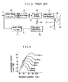
- Fig. 3 shows a conventional video signal, magnetic recording circuit for use in a VTR for home use of, for example, VHS type.
- a video signal h is separated into a luminance signal j and a chroma signal k by means of a low-pass filter 10 (hereinafter simply referred to as LPF) and a band-pass filter 11 (hereinafter simply referred to as BPF).
- LPF low-pass filter
- BPF band-pass filter 11
- the luminance signal j is FM-modulated by an FM modulator circuit 12 and thereafter fed to a mixer circuit 14 via a level adjuster 13.
- the chroma signal k is subjected to a low-band conversion by a low-band conversion circuit 15 and then fed to the mixer circuit 14 via a level adjuster 16.
- These signals are mixed together at the mixer circuit 14 and then passed to a resistor 19 which is grounded via an amplifier circuit 17 for recording and a magnetic head 18 by way of which a resultant mixed signal is recorded on a magnetic tape 20.
- the level adjusters 13 and 16 are monitored for level adjustment by using a signal delivered out of an output terminal 21.
- Fig. 4 shows graphically a specific example of recording current characteristics which is described in " VT R" by Kenichi Sawazaki, Corona-sha, p 49, Fig. 4.12, October, 1971.
- abscissa represents recording current passed through the magnetic head 18 and ordinate represents reproduced output level. It will be seen from Fig. 4 that changes in the recording current has an effect upon level and frequency characteristic of the reproduced output signal. Accordingly, a deviation of the recording current from an optimum value results in a degraded signal to noise ratio of a picture reproduced by the VTR.
- the recording current in the magnetic head 18 is adjusted by the level adjusters 13 and 16 so as to absorb fluctuations in the recording current due to variations in the impedance of magnetic head 18 and the circuit gain.
- the level adjuster 13 is so adjusted manually as to make a voltage drop across the resistor 19 developing at the output terminal 21 correspond to an optimum value for a magnetic head used, and for the chroma signal k, the level adjuster 16 is manually adjusted such that the recording current exclusive: of the luminance signal, which results in a flow of only chroma signal drawn into the magnetic head, is usually flower than the level of the recording current inclusive of only the luminance signal by about 10 d B by which occurrence of cross-beat interference between the chroma arnd luminance signals can be avoided.
- the recording current In the VTR, the recording current must be adjusted manually in respect of both the luminance signal and chroma signal in this manner and the troublesome adjustment can be effectuated only by using the variable resistors which are costly.
- Fig. 5 shows an embodiment in which the invention is applied to a voice signal, magnetic recording apparatus such as VTR or tape recorder.
- a bias oscillator 22 whose oscillation magnitude is controllable is connected to a magnetic head 4 via a DC blocking capacitor 2.
- the magnetic bead 4 is grounded via a resistor 5.
- a voice signal to be recorded is supplied to an input terminal 7 and fed to an amplifier 8 at which it is amplified to a predetermined level and given a necessary frequency characteristic.
- An amplified voice signal delivered out of the amplifier 8 is passed through a DC blocking capacitor 9 and superimposed on a bias current i B .
- a resultant signal is recorded on a magnetic tape 6 by means of the magnetic head 4.
- the capacitors 4 and 9 have ends connected in common to the magnetic head and function to mix the voice signal and bias current.
- the amplifier 8, capacitors 2 and 9 and bias oscillator 22 constitute a voice signal processing circuit which converts the voice signal supplied to the input terminal 7 into a recording signal suitable for application to the magnetic head 4.
- An amplifier 23 has an input terminal connected to a junction between the resistor 5 and the magnetic head and an output terminal connected to an input terminal of a rectifier circuit 24.
- the rectifier circuit 24 has an output terminal connected to one input terminal of a control signal generator circuit 25, and a reference voltage source 26 of a voltage level V ref is connected between the other input terminal of the control signal generator circuit 25 and ground.
- the control signal generator circuit 25 has an output terminal connected to a control input terminal of the bias oscillator 22.
- a voltage v B developing across the resistor 5 in proportion to the bias current i B is amplified by the amplifier 23 to an appropriate level, and rectified and smoothed by the rectifier circuit 24 so as to be converted into a DC voltage signal which in turn is supplied to the one input terminal of the control signal generator circuit 25.
- the control signal generator 25 detects a difference between a level of the DC voltage signal and the preset voltage level V ref of the reference voltage source 26 and supplies to the control input terminal of the bias oscillator 22 a control signal adapted to cancel out the voltage level difference.
- the output signal level of the bias oscillator 22 is controlled by the control signal so as to set the bias current i B to a predetermined optimum value designated by the reference voltage source 26.
- the adjustment step for the bias current conventionally required in the production line of magnetic recording and reproducing apparatus can be dispensed with and it suffies to do away with the conventional design which necessarily takes into consideration the layout of the adjustable parts, thereby improving the degree of freedom of design.
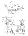
- the Fig. 5 magnetic recording circuit can be exemplarily implemented as shown in Fig. 6.
- a circuit corresponding to the amplifier circuit 23 shown in Fig. 5 comprises capacitors 27 and 33, an amplifier 28, resistors 30, 31 and 32, and a voltage source 29.
- a circuit corresponding to the rectifier circuit 24 shown in Fig. 5 comprises an NPN type transistor 34, a resistor 36, and a capacitor j7.
- a circuit corresponding to the Fig. 5 control signal generator circuit 25 comprises an amplifier 38, resistors 39, 40 and 42, and a transistor 41.
- a circuit corresponding to the Fig. 5 bias oscillator 22 comprises resistors 44 and 45, an NPN transistor 43, a voltage source 46 and an oscillator 100.
- a junction between the resistor 5 and the magnetic head 4 is connected to a non-inverting input terminal of the amplifier 28 via the DC blocking capacitor 27, and a voltage v B which results from the bias current i B superimposed with the voice signal and which develops across the resistor 5 is supplied to the non-inverting input terminal of the amplifier 28 via the DC blocking capacitor 27.
- the non-inverting input terminal is also connected to the voltage source 29 via the resistor 30.
- a DC voltage of this voltage source 29 causes the central level of the voltage v B to shift to a given level which lies within a range of input voltage over which the amplifier 28 is operable.
- the amplifier 28 has a gain determined by the resistors 31 and 32 and DC full feedback capacitor 33.
- the capacitor 33 also acts to prevent the DC voltage of the voltage source 29 from being amplified by the amplifier 28.
- An output terminal of the amplifier 28 is connected to a base of the transistor 34 and the voltage v B , now amplified to a predetermined level by the amplifier 28, is supplied to the transistor 34.
- the transistor 34 has its collector connected to a power supply 35 and its emitter connected to a parallel connection of the resistor 36 and.capacitor 37, thereby completing an emitter follower detector circuit.
- a signal fed from the amplifier 28 is rectified by this circuit and led to a non-inverting input terminal of the amplifier 38.
- the amplifier 38 is connected with the resistors 39 and 40 for gain setting and is also connected, at its inverting input terminal, to the reference voltage source 26 via the resistor 40.
- An output terminal of the differential amplifier 38 is connected to a base of the transistor 41. A difference between the level of the signal applied to the non-inverting input terminal and the voltage V ref of the reference voltage source 26 is detected, and the difference is amplified to a predetermined level and then supplied to the transistor 41.
- the transistor 41 has its emitter grounded via the resistor 42 and its collector connected to a base of the transistor 43.
- the base of the transistor 43 is grounded via the resistor 44 and is connected via the resistor 45 to a collector of the transistor 43 and to the voltage source 46.
- the transistor 41 is responsive to a level of the voltage signal fed from the amplifier 38 to control base voltage of the transistor 43.
- collector current of the transistor 41 is I
- voltage of the voltage source 46 is V
- emitter voltage of the transistor 43 is V' cc
- resistance of the resistor 45 is R
- forward base-emitter voltage is V F
- the emitter voltage V' cc is used as a power supply voltage for feeding the bias oscillator 100 so that the output signal level of the bias oscillator 100 is variable in proportion to this emitter voltage V' cc .
- the bias current i B increases and consequently the voltage v B developing across the resistor 5 increases, with the result that a higher voltage than the voltage V ref of the reference voltage source 26 is supplied to the differential amplifier 38.
- the output signal level of the differential amplifier 38 increases, followed by an increase in the collector current I1 of the transistor 41. It follows therefore pursuant to the above equation (1) that the power supply voltage or emitter voltage V' CC decreases to reduce the output signal level of the bias oscillator 100, thereby maintaining the bias current i B at the predetermined value.
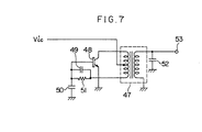
- Fig. 7 is a circuit diagram showing an example of the oscillator 100 of Fig. 6.
- the emitter voltage V I cc is led to a center tap of a primary winding of a bias transformer 47.
- One end of the primary winding of the bias transformer 47 is connected to a collector of a transistor 48.
- the transistor 48 has its emitter grounded and its base connected to one end of each of the capacitors 49 and 50 and a resistor 51.
- the other end of the capacitor 50 is grounded.
- the other end of each of the capacitor 49 and resistor 51 is connected to the other end of the primary winding of the bias transformer 47.
- the bias transformer 47 has a secondary winding of which one end is grounded and the other end is connected to one end of a capacitor 52 and to an output terminal 53. The other end of the capacitor 52 is grounded.
- the oscillation output appears at the output terminal 53.
- the resistor 51 acts as a base bias resistor for the transistor 48, the capacitors 49 and 50 determine the amount of A C signal feedback to the base of the transistor 48, and the capacitor 52 cooperates with an inductance of the secondary winding of the bias transformer 47 to determine the oscillation frequency.
- the oscillator 100 constructed as above generates an oscillation output whose level is controlled by the emitter voltage VI cc .
- the oscillator 100 is in no way limited to the oscillator shown in Fig. 7 but it may obviously be any types of oscillator whose output is controllable.
- Fig. 8 shows an embodiment in which the invention is applied to a video signal, magnetic recording apparatus.
- an input terminal 54 is for reception of a video signal h, and the LPF 10, BP F 11, FM modulator circuit 12, low-band conversion circuit 15, mixer circuit. 14 and recording amplifier circuit 17 constitute sa recording signal processing section.
- a current controlled -type amplifier circuit (hereinafter simply referred to as CCA circuit) 55 is inserted between the FM modulator c-ircuit 12 for FM modulation of a luminance signal j anrd the mixer circuit 14.
- a CCA circuit 56 is inserted between the low-band conversion circuit 15 for low-banrd conversion of a chroma signal k and.the mixer circuit 14.
- the CCA circuits control the recording signal processing section so as to adjust the levels of the luminance signal and chroma signal.
- these CCA circuits operate to respond to changes in a control signal Icont so as to change the levels of the luminance signal and the chroma signal based on the fact that the control signal I cont is related to an input/ output gain G of the CCA circuit by I cont « G.
- a voltage signal representative of a recording current developing across the resistor 19 is, on the other hand, inputted to a recording signal control section 57 depicted by a chained line block, and an output signal of this section 57 is supplied as the control signal I cont to the CCA circuits 55 and 56.
- the voltage signal detected from the resistor 19 is first applied to a high-pass filter (hereinafter simply referred to as HPF) 58 which passes only a signal indicative of a luminance signal component contained in the recording current flowing through the magnetic head 18, and the luminance component signal is fed to a gate circuit 84 which extracts from the luminance component signal a sync signal component.
- HPF high-pass filter
- the gate circuit 84 is controlled by receiving an output of a sync signal separation circuit 83 which detects a sync signal from the video signal h.
- An output voltage of the gate circuit 84 is amplified by an amplifier circuit 59, rectified by a rectifier circuit 60 and then inputted to a comparator 61.
- the comparator 61 is also inputted with a reference voltage from a reference voltage source 62 for determination of a desired recording current, and a rectified voltage is compared with the reference voltage at the comparator 61. A resulting difference voltage is amplified by the comparator 61 and applied to a voltage-to-current converter (or simply referred to as V/I circuit) 63.
- V/I circuit voltage-to-current converter
- an output current of the control section 57 which has been converted from the output voltage of the comparator 61 into a current corresponding to the output voltage value by the voltage-to-current converter 63, is supplied as a control signal I cont to the CCA circuits 55 and 56 to control the levels of the luminance signal and the chroma signal such that the recording signal flowing through the magnetic head 18 is constantly controlled to a desired value.
- control section 57 An example of the control section 57 is illustrated in a circuit diagram of Fig. 9 in which other elements than the control section are illustrated in block form.
- a recording current flowing through the magnetic head 18 causes a voltage drop across the resistor 19 and a voltage representative of the recording current is applied to one end of a capacitor 64.
- the other end of the capacitor 64 is grounded via a resistor 65.
- the capacitor 64 and the resistor 65 constitute the HPF 58.
- the voltage is then supplied to a base of a transistor 87 via a DC blocking capacitor 66.
- the base of the transistor 87 is fed with a DC bias voltage from a bias voltage source 68 via a resistor 69.
- the transistor 87 has its collector connected to a power supply 74 and its emitter connected to a collector of a transistor 88 and to a cathode of a diode 89.
- An anode of the diode 89 is connected to one end of a resistor 90 and a non-inverting input terminal of an amplifier 67.
- the other end of the resistor 90 is connected to the power supply 74.
- the transistor 88 cooperates with its emitter resistor 91 to constitute a constant current circuit as will be described later.
- This transistor 88 has its base controlled by the output of the sync signal separation circuit 83.
- the gate circuit 84 transmits the output of the HPF 58 to the succeeding stage of amplifier circuit 59 when the output of the sync signal separation circuit 83 is present but does not do so when the output of the sync signal separation circuit is grounded.
- the output of the sync signal separation circuit 83 is a sync signal extracted from the video signal h, and the gate circuit 84 is controlled by this sync signal so that only the sync signal contained in the luminance signal component of the recording current flowing through the magnetic head 18 can be derived.
- the sync signal separated from the video signal h by means of the sync signal separation circuit 83 is a signal of a constant voltage. Therefore, the emitter voltage of the transistor 88 is a constant voltage which is lower than the constant voltage of sync signal by a base-emitter voltage V BE of the transistor 88. Emitter current of the transistor 88 is then obtained by dividing the emitter voltage by a resistance of the resistor 91 and it becomes a constant current value, providing a constant collector current. Accordingly, the transistor 88 and resistor 91 constitute the constant current circuit as mentioned previously.
- the gate circuit 84 when the transistor 88 is turned on by the sync signal, the diode 89 is also turned on and its anode potential becomes substantially equal to a base potential of the transistor 87, with the result that a level of the sync signal detected by the resistor 19 is transmitted to a non-inverting input terminal of succeeding stage amplifier 67 which is connected to the anode of the diode 89.
- an output terminal of the amplifier 67 is connected via a resitor 70 to an inverting input terminal, and a resistor 71 and a DC full feedback capacitor 72 are connected between the inverting input terminal and ground.
- the closed circuit gain of the amplifier 67 i.e., the gain of the amplifier circuit 59 is determined by the resistors 70 and 71.
- the output terminal of the amplifier 67 is connected to a base of a transistor 73.
- the transistor 73 has its collector connected to the power supply 74 and its emitter connected to resistors 75 and 77 and a capacitor 76.
- the transistor 73, resistor 75 and capacitor 76 constitute an emitter follower detector circuit which rectifies and smoothes the output voltage of the amplifier 67 to provide a DC voltage.
- the other end of the resistor 77 is connected to an inverting input terminal of an amplifier 78 and to one end of a resistor 79.
- the other end of the resistor 79 is connected to an output terminal of the amplifier 78.
- An non-inverting input terminal of the amplifier 78 is supplied from a reference voltage source 62 with a reference voltage which corresponds to the desired value of the recording current flowing through the magnetic head 18.
- a difference voltage between an emitter voltage of the transistor 73 and the reference voltage is amplified in accordance with a gain determined by the resistors 77 and 79 to provide an output voltage of the amplifier 78.
- the output voltage of the amplifier 78 is decreased when the emitter voltage of the transistor 73 exceeds the reference voltage and is increased when the emitter voltage is below the reference voltage.
- An output terminal of the amplifier 78 is connected to a base of a transistor 80.
- the transistor 80 has its emitter grounded via a resistor 81 and its collector connected to the CCA circuits 55 and 56.
- An output voltage of the amplifier 78 is converted into a control current I cont in accordance with an emitter voltage of the transistor 80 and a resistance of the resistor 81.
- the control signal I cont changes the gain of the CCA circuits 55 and 56 to thereby change the levels of the luminance signal and the chroma signal.
- the amplifier circuit 59, rectifier circuit 60, comparator 61 and V/I circuit (voltage-to-circuit converter) 63 described above have essentially the same construction as that of the amplifier circuit 23, rectifier circuit 24 and control circuit 25.
- Fig. 10 showing an example of the CCA circuit, it will be detailed how the gain of the CCA circuit changes with the control signal I cont .
- a signal source 92 is representative of the output signal of the FM modulation circuit 12 and/or the low-band conversion circuit 15 shown in Fig. 8 or 9.
- An output terminal 124 of the CCA circuit is adapted to be connected to an input terminal of the mixer circuit 14.
- An input signal Vi from the signal source 92 is applied to a base of a transistor 94 via a DC blocking capacitor 93.
- the base of the transistor 94 is supplied via a bias resistor 95 with a DC bias from the bias voltage source 68 (identical to that of Fig. 9 but illustrated herein for ease of understanding).
- the DC bias is also applied via a bias resistor 97 to a base of a transistor 96 which constitutes together. with the transistor 94 a first stage of differential amplifier. Emitters of the transistors 94 and 96 are mutually connected via resistors 98 and 99 each having a resistance of R E . A constant current of I is caused by an constnat current source 110 to flow between a junction of the resistors 98 and 99 and ground.
- Collectors of the transistors 94 and 96 are respectively connected to cathodes of diodes 111 and 112 in order that operating resistances of these diodes are used as loads on the transistors 94 and 96.
- Anodes of the diodes 111 and 112 are connected in common to a cathode of a diode 113 adapted for DC voltage shifting.
- the diode 113 has its anode connected to the power supply line 74.
- the collectors of the transistors 94 and 96 are also connected respectively to bases of transistors 114 and 115 which constitute a second stage of differential amplifier. Emitters of the transistors 114 and 115 are connected in common to a variable constant current source 116. By controlling a constant current I cont of the constant current source 116, the gain of the CCA circuit can be changed.
- the transistor 114 has its collector connected to collector and base of a transistor 117.
- the base of the transistor 117 is connected to a base of a transistor 118 to constitute a current mirror circuit.
- the transistor 115 has its collector connected to collector and base of a transistor 119.
- the base of the transistor 119 is connected to a base of a transistor 120 to constitute a current mirror circuit.
- the signal Vi is derived from the transistors 118 and 120 as changes in collector currents of the transistors 118 and 120.
- Transistors 121 and 122 have their bases mutually connected to form a current mirror circuit.
- the transistor 121 has its collector connected to a collector of the transistor 118 and the transistor 122 has its collector connected to a collector of the transistor 120.
- the collectors of the transistors 120 and 122 are connected in common to a load resistor 123 of a resistance of R L connected to the bias voltage source 68.
- An output signal current i 0 flows through the load resistor 123 and is converted into an output signal voltage V .
- collector current of the transistor 114 having the base at the same potential as that at the collector of the transistor 94 is decreased while collector current of the transistor 115 having the base at the same potential as that at the collector of the transistor 96 is increased.
- an amount of decrement in the collector current of the transistor 114 results in an amount of increment in the collector current of the transistor 115, giving rise to the increased collector current of the transistor 115.
- collector current of the transistor 114 is identical to emitter current of the transistor 117 and the transistors 117 and 118 form the current mirror circuit, collector currents of the transistors 114 and 118 are equal to each other. Since the collector current of the transistor 115 is identical to emitter current of the transistor 119 and the transistors 119 and 120 form the current mirror circuit, collector currents of the transistors 115 and 120 are equal to each other. Further the transistors 121 and 122 forming the current mirror circuit have the same collector current and collector current of the transistor 121 is identical to collector current of the transistor 118. For these reasons, collector current of the transistor 122 eventually becomes equal to the collector current of the transistor 114.
- the collector current of the transistor 114 decreases while the collector current of the transistor 115 increases, the collector current of the transistor 120 is increased while the collector current of the transistor 122 is decreased.
- the difference between the collector currents of the transistors 120 and 122 is given as an output current i 0 which flows through the load resistor 123, generating an output voltage v o . It will be appreciated from the foregoing description that the transistor 120 acts to supply the output current i o to the load resistor 123 and the transistor 122 acts to draw the output current i .
- the CCA circuit configured as above has the input/output gain as will be calculated below. It is now assumed that the transistors 94 and 96 have each an emitter operating resistance r e0 , the diodes 111 and 112 have each an operating resistance r e1' and the transistors 114 and 115 have each an emitter operating resistance re2.
- the circuit (input/output) gain G of 10 the CCA circuit is given by, In equation (6), , R e , I o and R L are fixed and there results where indicating that the input/ output gain G of the CCA circuit changes in proportion to the control signal I cont .
- the impedance of the magentic head 18 is larger with the recording current decreased, then the detection voltage from the resistor 19 will be decreased and the output of the rectifier circuit 60 will be decreased.
- This output of the rectifier circuit 60 is compared at the comparator circuit 61 with the reference voltage of reference voltage source 62 corresponding to the predetermined recording current.
- the output voltage of the comparator circuit 61 is raised to increase the control current for the CCA circuits 55 and 56.
- the circuit (input/output) gain of the CCA circuits 55 and 56 is raised to increase the output signal level of the CCA circuits 55 and 56, thereby increasing the recording current to the predetermined constant value.
- the impedance of the magnetic head 18 is smaller with the recording current increased, then the detection voltage from the resistor 19 will be increased and the outputt of the rectifier circuit 60 will be increased.
- This output of the rectifier circuit 60 exceeds the reference voltage of the reference voltage source 62 and hence the output voltacge of the comparator circuit 61 is decreased to reduce the control current for the CCA circuits 55 and 56.
- the circuit gain of the CCA circuits 55 and 56 is decreased to reduce the output signal level of the CCA circuits 55 and 56, thereby decreasing the recording current to the predetermined constant value.
- a desired level difference between the luminance and chroma signals of the recording current can be provided readily by selecting, at an initial circuit design phase, either the constant current I o of the initial-stage differential amplifier or the load resistance R L of the CCA circuits so as to provide a desired gain difference.
- Fi g . 11 shows, in block form, another embodiment in which the invention is applied to a video signal, magnetic recording apparatus.
- the Fig. 11 embodiment contemplates control of the chroma signal of the recording current by detecting a burst signal of the chroma signal.
- a voltage developing across the resistor 19 is applied to a HPF 58 and a BPF 125 for detection of a chroma signal.
- An output signal of the BPF 125 is fed to a second gate circuit 86.
- the gate circuit 86 is controllable by an output of a gate pulse generator 85 which is supplied with a video signal h.
- the gate pulse generator 85 comprises a monostable multivibrator which is triggered by a burst signal contained in the video signal.
- the monostable multivibrator is so set as to produce a high level output signal over a time interval corresponding to a period of the burst signal contained in the video signal, and during the time interval, the gate circuit 86 is enabled to pass therethrough the signal inputted thereto.
- the gate circuit 86 is therefore adapted for extraction of the burst signal from the chroma signal of the recording signal flowing through the magnetic head 18.
- the output signal of the gate circuit 86 is amplified by an amplifier circuit 126, rectified and smoothed by a rectifier circuit 127 and then supplied to a comparator 128.
- the comparator 128 is also supplied from a reference voltage source 129 with a reference voltage corresponding to a predetermined level of the chroma signal of the recording current.
- a rectified and smoothed DC voltage is compared with the reference voltage and a resulting difference voltage is amplified.
- This difference voltage is converted by a V/I circuit (voltage-to-current converter) 130 into a current which is used as a control signal applied to the CCA circuit 56 adapted for level change of the chroma signal so as to control the chroma signal of the recording current.
- V/I circuit voltage-to-current converter
- the chroma signal control section can be implemented by using circuits similar to those of the luminance signal control section 57.
- variable resistors for adjustment of the luminance and chroma signals of the recording current in the recording circuit of the magnetic recording and reproducing apparatus, thereby eliminating steps for adjustment of the recording current.
- Fig. 12 shows, in block form, a further embodiment in which the invention is applied to a recording circuit of an apparatus for recording and reproducing frequency modulated voice signals.
- an input terminal 131 is for a voice AM signal of right channel (hereinafter referred to as Rch) and an input termianl 132 is for a voice AM signal of left channel (hereinafter referred to as Lch).
- An input signal received by the input terminal 131 is FM modulated by an FM modulator 133, amplified by a CCA circuit 134 to a level designated by an output of a voltage-to-current converter 145 and then supplied to a mixer circuit 135.
- An input signal received by the input terminal 132 is FM modulated by an FM modulator 136, amplified by a CCA circuit 137 to the level designated by the output of the voltage-to-current converter 145 and then supplied to the mixer circuit 135.
- An output signal of the mixer circuit 135 is supplied via a recording signal amplifier circuit 138 to a magnetic head 139 for recording of voice signals and recorded on a magnetic tape 20.
- a recording current flowing through the magnetic head 139 is detected by a resistor 19, and a detection signal is passed through a HPF 140 (LPF may substituted for the HPF depending on which of Rch or Lch of the voice carrier frequency is extracted) so that a predetermined channel signal is extracted from the detection signal.
- the extracted channel signal is amplified by an amplifier circuit 141, rectified and smoothed by a rectifier circuit 142 so as to be converted into a DC voltage which in turn is compared at a comparator 143 with a reference voltage of a reference voltage source 144.
- the reference voltage corresponds to a desired recording current.
- a resulting difference voltage is amplified in the comparator and converted by a voltage-to current converter 145 into a current which is used to control the CCA circuits 134 and 137.
- the level of the FM modulated signal like the video signal of the recording current, is so controlled as to keep constant the recording current of the magnetic head 139.
Abstract
Description
- The present invention relates to a recording circuit in a magnetic recording and reproducing apparatus and more particularly to a magnetic recording circuit suitable for use as a recording circuit for video signals in a video tape recorder (VTR) of, for example, a helical scan type, a recording circuit of a voice FM recording and reproducing apparatus or a bias current circuit for controlling a bias current supplied to a recording head of a tape recorder.
- A magnetic recording and reproducing apparatus such as a VTR or a tape recorder has in its recording circuit for voice signals a bias current circuit and for recording a voice signal, the voice signal is superimposed on a bias current in order that upon reproduction of the voice signal, waveform distortions can be suppressed. However, where the bias current supplied to a magnetic head does not have a proper value, the reproduced voice signal will be degraded in its frequency characteristics, decreased in its level and accompanied by an increased waveform distortion. To cope with this problem, it is a practice to provide in the bias current circuit a variable resistor for adjustment of level of the bias current. In mass production of magnetic recording and reproducing apparatus, for individual products, the level adjustment by by means of the variable resistor is undertaken which is very time-consuming and troublesome. In addition, for ease of the adjustment, layout of the variable resistor must be taken into consideration and the degree of freedom of design is impaired.
- An object of this invention is to provide a magnetic recording circuit which can automatically set current signals passed through a magnetic head to a predetermined level without resort to a variable resistor for adjustment of level of the current signals.
- To accomplish the above object, according to an aspect of this invention, there is provided a magnetic recording apparatus for recording information on a recording medium through a magnetic head having a predetermined recording characteristic, comprising recording signal processing means receiving an input signal representative of information to be recorded, for processing the received input signal so as to generate a recording signal of a given level to be supplied to the magnetic head; means for detecting the recording signal passed through the magnetic head; control signal generation means, responsive to the detected recording signal, for generating a control signal adapted for setting the level of the recording signal passed through the magnetic head to a predetermined level; and control means, responsive to the control signal, for controlling the recording signal processing means so as to set the recording signal passed through the magnetic head to the predetermined set level.
-
- Fig. 1 is a circuit diagram showing an example of a conventional bias current circuit.
- Fig. 2 is a graph showing bias characteristics of a magnetic head.
- Fig. 3 is a block diagram showing a video signal recording circuit of a conventional VTR for home use.
- Fig. 4 is a graph showing recording current versus reproduction output characteristics of the VTR magnetic head with frequencies used as parameters.
- Fig. 5 is a block diagram of a magnetic recording circuit for a voice signal according to an embodiment of the invention.
- Fig. 6 is a circuit diagram of a circuit arrangement for implementation of the Fig. 5 embodiment.
- Fig. 7 is a circuit diagram of a circuit arrangement for implementation of a bias oscillator shown in Fig. 6.
- Fig. 8 is a block diagram of a magnetic recording apparatus for a voice signal according to an embodiment of the invention.
- Fig. 9 is a circuit diagram showing a partial circuit arrangement for implementation of the magnetic recording apparatus shown in Fig. 8.
- Fig. 10 is a circuit diagram of a circuit arrangement for implementation of a current controlled type amplifier (CCA) used in the embodiment of Fig. 9.
- Fig. 11 is a block diagram showing another embodiment of a magnetic recording apparatus for a video signal according to the invention.
- Fig. 12 is a block diagram showing an embodiment in which the invention is applied to a FM modulation magnetic recording apparatus for a voice signal.
- Prior to describing the invention by way of example with reference to the accompanying drawings, a conventional magnetic recording apparatus will first be described by referring to Figs. 1 to 4, for better understanding of the invention.
- A conventional bias current circuit for use in a tape recorder as examplified in Fig. 1 comprises a bias oscillator 1,
capacitors 2 and 9, avariable resistor 3, aresistor 5, an input erminal 7, and anamplifier 8. Amagnetic head 4 associated with amagnetic tape 6 is connected between thevariable resistor 3 and theresistor 5. - In Fig. 1, a bias signal generated from the bias oscillator 1 is passed through the
DC blocking capacitor 2 and converted into a bias current iB of a value determined by a resistance of thevariable resistor 3. The bias current i Bis drawn to an ground terminal via a winding of themagnetic head 4 and theresistor 5. - A voice signal, on the other hand, is applied to the
input terminal 7 and fed to theamplifier 8 at which it is amplified to a predetermined level and given a desired frequency characteristic for the purpose of amplitude and phase equalization and high-frequency band correction and the like. An output voice signal delivered out of theamplifier 8 is passed through the DC blocking capacitor 9 so as to be superimposed on the bias current iB and recorded on themagnetic tape 6 by means of themagnetic head 4. - The bias current circuit of the above construction which is based on AC bias recording can minimize waveform distortions accompanying recording signals and therefore, it has been used in many applications.
- Fig. 2 graphically shows bias characteristics for a magnetic head of tape recorder.
- In Fig. 2, abscissa represents bias current, lefthand ordinate represents reproduced output level and righthand ordinate represents distortion factor. For recording signals at various predetermined frequencies, changes in the reproduced output level are plotted with respect to changes in the bias current to provide characteristic curves a to e, and for a recording signal at a predetermined frequency, changes in the distortion factor with respect to changes in the bias current are plotted to provide a characteristic curve g.
- As will be seen from Fig. 2, for improper values of the bias current, the reproduced output level changes to a large extent, and frequency characteristics and distortion factor characteristics are degraded.
- The bias current deviates from an optimum value due to the fact that the level of the bias signal outputted from the bias oscillator 1 fluctuates and the impedance of one magnetic head is slightly different from that of another magnetic head.
- Conventionally, a voltage drop vB across the
resistor 5 shown in Fig. 1 is therefore measured to detect an amount of bias current, and thevariable resistor 3 is then set through manual adjustment to a value which makes the voltage drop v developing across theresistor 5 correspond to the optimum value of the bias current. - An example resembling the conventional bias current circuit shown in Fig. 1 is disclosed in "Tape Recorder" by Okiaki Tsuno, Nikkan Kohgyo Shimbun-sha, pp 71-72, April, 1971.
- A video signal, magnetic recording circuit of VTR will now be described.
- Fig. 3 shows a conventional video signal, magnetic recording circuit for use in a VTR for home use of, for example, VHS type. In Fig. 3, a video signal h is separated into a luminance signal j and a chroma signal k by means of a low-pass filter 10 (hereinafter simply referred to as LPF) and a band-pass filter 11 (hereinafter simply referred to as BPF). The luminance signal j is FM-modulated by an
FM modulator circuit 12 and thereafter fed to amixer circuit 14 via alevel adjuster 13. The chroma signal k is subjected to a low-band conversion by a low-band conversion circuit 15 and then fed to themixer circuit 14 via alevel adjuster 16. These signals are mixed together at themixer circuit 14 and then passed to aresistor 19 which is grounded via anamplifier circuit 17 for recording and amagnetic head 18 by way of which a resultant mixed signal is recorded on amagnetic tape 20. Thelevel adjusters output terminal 21. - Fig. 4 shows graphically a specific example of recording current characteristics which is described in "VTR" by Kenichi Sawazaki, Corona-sha,
p 49, Fig. 4.12, October, 1971. In Fig. 4, abscissa represents recording current passed through themagnetic head 18 and ordinate represents reproduced output level. It will be seen from Fig. 4 that changes in the recording current has an effect upon level and frequency characteristic of the reproduced output signal. Accordingly, a deviation of the recording current from an optimum value results in a degraded signal to noise ratio of a picture reproduced by the VTR. - To cope with this problem, in the VTR for home use, the recording current in the
magnetic head 18 is adjusted by thelevel adjusters magnetic head 18 and the circuit gain. - To this end, for the luminance signal j, the
level adjuster 13 is so adjusted manually as to make a voltage drop across theresistor 19 developing at theoutput terminal 21 correspond to an optimum value for a magnetic head used, and for the chroma signal k, the level adjuster 16 is manually adjusted such that the recording current exclusive: of the luminance signal, which results in a flow of only chroma signal drawn into the magnetic head, is usually flower than the level of the recording current inclusive of only the luminance signal by about 10 dB by which occurrence of cross-beat interference between the chroma arnd luminance signals can be avoided. - In the VTR, the recording current must be adjusted manually in respect of both the luminance signal and chroma signal in this manner and the troublesome adjustment can be effectuated only by using the variable resistors which are costly.
- An example of a circuit confugration similar to the abova recording current adjustment circuit is disclosed in "Compact VTR" by Masakazu Hara and Saburo Takahashi, Nippon HOso Shuppan Kyokai,
p 93, March, 1972. - The invention will now be described by way of example with reference to the drawings. In the following description. identical elements to those of Figs. 1 and 3 are designated by identical reference numerals and will not be detailed:
- Fig. 5 shows an embodiment in which the invention is applied to a voice signal, magnetic recording apparatus such as VTR or tape recorder. In Fig. 5, a bias oscillator 22 whose oscillation magnitude is controllable is connected to a
magnetic head 4 via aDC blocking capacitor 2. Themagnetic bead 4 is grounded via aresistor 5. A voice signal to be recorded, on the other hand, is supplied to aninput terminal 7 and fed to anamplifier 8 at which it is amplified to a predetermined level and given a necessary frequency characteristic. An amplified voice signal delivered out of theamplifier 8 is passed through a DC blocking capacitor 9 and superimposed on a bias current iB. A resultant signal is recorded on amagnetic tape 6 by means of themagnetic head 4. Thecapacitors 4 and 9 have ends connected in common to the magnetic head and function to mix the voice signal and bias current. Theamplifier 8,capacitors 2 and 9 andbias oscillator 22 constitute a voice signal processing circuit which converts the voice signal supplied to theinput terminal 7 into a recording signal suitable for application to themagnetic head 4. - An
amplifier 23 has an input terminal connected to a junction between theresistor 5 and the magnetic head and an output terminal connected to an input terminal of arectifier circuit 24. Therectifier circuit 24 has an output terminal connected to one input terminal of a controlsignal generator circuit 25, and areference voltage source 26 of a voltage level Vref is connected between the other input terminal of the controlsignal generator circuit 25 and ground. The controlsignal generator circuit 25 has an output terminal connected to a control input terminal of thebias oscillator 22. - In operation, a voltage vB developing across the
resistor 5 in proportion to the bias current iB is amplified by theamplifier 23 to an appropriate level, and rectified and smoothed by therectifier circuit 24 so as to be converted into a DC voltage signal which in turn is supplied to the one input terminal of the controlsignal generator circuit 25. - The
control signal generator 25 detects a difference between a level of the DC voltage signal and the preset voltage level Vref of thereference voltage source 26 and supplies to the control input terminal of the bias oscillator 22 a control signal adapted to cancel out the voltage level difference. - Thus, the output signal level of the
bias oscillator 22 is controlled by the control signal so as to set the bias current iB to a predetermined optimum value designated by thereference voltage source 26. - Since the predetermined optimum bias current iB can be set automatically in this manner, the adjustment step for the bias current conventionally required in the production line of magnetic recording and reproducing apparatus can be dispensed with and it suffies to do away with the conventional design which necessarily takes into consideration the layout of the adjustable parts, thereby improving the degree of freedom of design.
- The Fig. 5 magnetic recording circuit can be exemplarily implemented as shown in Fig. 6.
- Referring to Fig. 6, a circuit corresponding to the
amplifier circuit 23 shown in Fig. 5 comprisescapacitors amplifier 28,resistors voltage source 29. - A circuit corresponding to the
rectifier circuit 24 shown in Fig. 5 comprises anNPN type transistor 34, aresistor 36, and a capacitor j7. - A circuit corresponding to the Fig. 5 control
signal generator circuit 25 comprises an amplifier 38,resistors transistor 41. - A circuit corresponding to the Fig. 5
bias oscillator 22 comprisesresistors NPN transistor 43, avoltage source 46 and anoscillator 100. - A junction between the
resistor 5 and themagnetic head 4 is connected to a non-inverting input terminal of theamplifier 28 via theDC blocking capacitor 27, and a voltage vB which results from the bias current iB superimposed with the voice signal and which develops across theresistor 5 is supplied to the non-inverting input terminal of theamplifier 28 via theDC blocking capacitor 27. The non-inverting input terminal is also connected to thevoltage source 29 via theresistor 30. A DC voltage of thisvoltage source 29 causes the central level of the voltage vB to shift to a given level which lies within a range of input voltage over which theamplifier 28 is operable. Theamplifier 28 has a gain determined by theresistors full feedback capacitor 33. Thecapacitor 33 also acts to prevent the DC voltage of thevoltage source 29 from being amplified by theamplifier 28. - An output terminal of the
amplifier 28 is connected to a base of thetransistor 34 and the voltage vB, now amplified to a predetermined level by theamplifier 28, is supplied to thetransistor 34. - The
transistor 34 has its collector connected to apower supply 35 and its emitter connected to a parallel connection of theresistor 36and.capacitor 37, thereby completing an emitter follower detector circuit. A signal fed from theamplifier 28 is rectified by this circuit and led to a non-inverting input terminal of the amplifier 38. By setting a time constant of theresistor 36 andcapacitor 37 to be sufficiently greater than an oscillation period of theoscillator 100, a smoothed DC voltage having a level corresponding to a peak value of the amplified voltage v can be obtained. - The amplifier 38 is connected with the
resistors reference voltage source 26 via theresistor 40. An output terminal of the differential amplifier 38 is connected to a base of thetransistor 41. A difference between the level of the signal applied to the non-inverting input terminal and the voltage Vref of thereference voltage source 26 is detected, and the difference is amplified to a predetermined level and then supplied to thetransistor 41. - The
transistor 41 has its emitter grounded via theresistor 42 and its collector connected to a base of thetransistor 43. - The base of the
transistor 43 is grounded via theresistor 44 and is connected via theresistor 45 to a collector of thetransistor 43 and to thevoltage source 46. - The
transistor 41 is responsive to a level of the voltage signal fed from the amplifier 38 to control base voltage of thetransistor 43. - Assuming that collector current of the
transistor 41 is I,, voltage of thevoltage source 46 is V , emitter voltage of thetransistor 43 is V'cc , resistance of theresistor 45 is R, and forward base-emitter voltage is VF, there results
bias oscillator 100 so that the output signal level of thebias oscillator 100 is variable in proportion to this emitter voltage V'cc. - When the impedance of the
magnetic head 4 used is larger than a stipulated value by an excess according to which the bias current iB is decreased, the voltage vB developing across theresistor 5 falls below a predetermined value. As a result, the signal level supplied to the differential amplifier 38 becomes lower than the voltage Vref of thereference voltage source 26 to thereby decrease collector current of thetransistor 41. It follows therefore pursuant to equation (1) that voltage drop across theresistor 45 is decreased to raise the emitter voltage V'cc and consequent output signal level of thebias oscillator 100. Consequently, the bias current iB can be maintained at an optimum value designated by thereference voltage source 26. - Conversely, when a
magnetic head 4 having a small impedance is used, the bias current iB increases and consequently the voltage vB developing across theresistor 5 increases, with the result that a higher voltage than the voltage Vref of thereference voltage source 26 is supplied to the differential amplifier 38. As a result, the output signal level of the differential amplifier 38 increases, followed by an increase in the collector current I1 of thetransistor 41. It follows therefore pursuant to the above equation (1) that the power supply voltage or emitter voltage V'CC decreases to reduce the output signal level of thebias oscillator 100, thereby maintaining the bias current iB at the predetermined value. - Fig. 7 is a circuit diagram showing an example of the
oscillator 100 of Fig. 6. The emitter voltage VI cc is led to a center tap of a primary winding of abias transformer 47. One end of the primary winding of thebias transformer 47 is connected to a collector of atransistor 48. Thetransistor 48 has its emitter grounded and its base connected to one end of each of thecapacitors resistor 51. The other end of thecapacitor 50 is grounded. The other end of each of thecapacitor 49 andresistor 51 is connected to the other end of the primary winding of thebias transformer 47. - The
bias transformer 47 has a secondary winding of which one end is grounded and the other end is connected to one end of a capacitor 52 and to anoutput terminal 53. The other end of the capacitor 52 is grounded. The oscillation output appears at theoutput terminal 53. Theresistor 51 acts as a base bias resistor for thetransistor 48, thecapacitors transistor 48, and the capacitor 52 cooperates with an inductance of the secondary winding of thebias transformer 47 to determine the oscillation frequency. Theoscillator 100 constructed as above generates an oscillation output whose level is controlled by the emitter voltage VI cc. - The
oscillator 100 is in no way limited to the oscillator shown in Fig. 7 but it may obviously be any types of oscillator whose output is controllable. - As described above, since according to this embodiment, feedback control is effected so as to maintain the bias current at the optimum value, the manual adjustment of the bias current can completely be dispensed with and it suffices in design of magnetic recording and reproducing apparatus to do away with consideration of the layout of the bias current adjusting means, thereby improving the degree of freedom of design. For these reasons, magnetic recording circuit for a voice signal with a bias current circuit can be provided which can eliminate the drawbacks of the conventional technique and perform an excellent function.
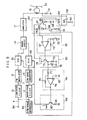
- Fig. 8 shows an embodiment in which the invention is applied to a video signal, magnetic recording apparatus.
- In Fig. 8, identical elements to those of Fig. 3 are designated by identical reference numerals and will not be detailed herein.
- preferring to Fig. 8, an
input terminal 54 is for reception of a video signal h, and theLPF 10, BPF 11, FMmodulator circuit 12, low-band conversion circuit 15, mixer circuit. 14 andrecording amplifier circuit 17 constitute sa recording signal processing section. A current controlled -type amplifier circuit (hereinafter simply referred to as CCA circuit) 55 is inserted between the FM modulator c-ircuit 12 for FM modulation of a luminance signal j anrd themixer circuit 14. Similarly, a CCA circuit 56 is inserted between the low-band conversion circuit 15 for low-banrd conversion of a chroma signal k and.themixer circuit 14. The CCA circuits control the recording signal processing section so as to adjust the levels of the luminance signal and chroma signal. As will be detailed later, these CCA circuits operate to respond to changes in a control signal Icont so as to change the levels of the luminance signal and the chroma signal based on the fact that the control signal Icont is related to an input/ output gain G of the CCA circuit by Icont « G. A voltage signal representative of a recording current developing across theresistor 19 is, on the other hand, inputted to a recordingsignal control section 57 depicted by a chained line block, and an output signal of thissection 57 is supplied as the control signal Icont to theCCA circuits signal control section 57, the voltage signal detected from theresistor 19 is first applied to a high-pass filter (hereinafter simply referred to as HPF) 58 which passes only a signal indicative of a luminance signal component contained in the recording current flowing through themagnetic head 18, and the luminance component signal is fed to agate circuit 84 which extracts from the luminance component signal a sync signal component. To this end, thegate circuit 84 is controlled by receiving an output of a syncsignal separation circuit 83 which detects a sync signal from the video signal h. An output voltage of thegate circuit 84 is amplified by anamplifier circuit 59, rectified by arectifier circuit 60 and then inputted to acomparator 61. Thecomparator 61 is also inputted with a reference voltage from areference voltage source 62 for determination of a desired recording current, and a rectified voltage is compared with the reference voltage at thecomparator 61. A resulting difference voltage is amplified by thecomparator 61 and applied to a voltage-to-current converter (or simply referred to as V/I circuit) 63. Thus, an output current of thecontrol section 57, which has been converted from the output voltage of thecomparator 61 into a current corresponding to the output voltage value by the voltage-to-current converter 63, is supplied as a control signal Icont to theCCA circuits magnetic head 18 is constantly controlled to a desired value. - An example of the
control section 57 is illustrated in a circuit diagram of Fig. 9 in which other elements than the control section are illustrated in block form. A recording current flowing through themagnetic head 18 causes a voltage drop across theresistor 19 and a voltage representative of the recording current is applied to one end of acapacitor 64. - The other end of the
capacitor 64 is grounded via aresistor 65. Thecapacitor 64 and theresistor 65 constitute theHPF 58. The voltage is then supplied to a base of atransistor 87 via aDC blocking capacitor 66. - The base of the
transistor 87 is fed with a DC bias voltage from abias voltage source 68 via aresistor 69. Thetransistor 87 has its collector connected to apower supply 74 and its emitter connected to a collector of atransistor 88 and to a cathode of adiode 89. An anode of thediode 89 is connected to one end of a resistor 90 and a non-inverting input terminal of anamplifier 67. The other end of the resistor 90 is connected to thepower supply 74. Thetransistor 88 cooperates with itsemitter resistor 91 to constitute a constant current circuit as will be described later. Thistransistor 88 has its base controlled by the output of the syncsignal separation circuit 83. Thegate circuit 84 transmits the output of theHPF 58 to the succeeding stage ofamplifier circuit 59 when the output of the syncsignal separation circuit 83 is present but does not do so when the output of the sync signal separation circuit is grounded. The output of the syncsignal separation circuit 83 is a sync signal extracted from the video signal h, and thegate circuit 84 is controlled by this sync signal so that only the sync signal contained in the luminance signal component of the recording current flowing through themagnetic head 18 can be derived. - The sync signal separated from the video signal h by means of the sync
signal separation circuit 83 is a signal of a constant voltage. Therefore, the emitter voltage of thetransistor 88 is a constant voltage which is lower than the constant voltage of sync signal by a base-emitter voltage VBE of thetransistor 88. Emitter current of thetransistor 88 is then obtained by dividing the emitter voltage by a resistance of theresistor 91 and it becomes a constant current value, providing a constant collector current. Accordingly, thetransistor 88 andresistor 91 constitute the constant current circuit as mentioned previously. To further detail the operation of thegate circuit 84, when thetransistor 88 is turned on by the sync signal, thediode 89 is also turned on and its anode potential becomes substantially equal to a base potential of thetransistor 87, with the result that a level of the sync signal detected by theresistor 19 is transmitted to a non-inverting input terminal of succeedingstage amplifier 67 which is connected to the anode of thediode 89. - In the
amplifier circuit 59, an output terminal of theamplifier 67 is connected via aresitor 70 to an inverting input terminal, and aresistor 71 and a DCfull feedback capacitor 72 are connected between the inverting input terminal and ground. With this construction, the closed circuit gain of theamplifier 67, i.e., the gain of theamplifier circuit 59 is determined by theresistors - The output terminal of the
amplifier 67 is connected to a base of atransistor 73. Thetransistor 73 has its collector connected to thepower supply 74 and its emitter connected toresistors capacitor 76. Thetransistor 73,resistor 75 andcapacitor 76 constitute an emitter follower detector circuit which rectifies and smoothes the output voltage of theamplifier 67 to provide a DC voltage. - The other end of the
resistor 77 is connected to an inverting input terminal of anamplifier 78 and to one end of aresistor 79. The other end of theresistor 79 is connected to an output terminal of theamplifier 78. An non-inverting input terminal of theamplifier 78 is supplied from areference voltage source 62 with a reference voltage which corresponds to the desired value of the recording current flowing through themagnetic head 18. A difference voltage between an emitter voltage of thetransistor 73 and the reference voltage is amplified in accordance with a gain determined by theresistors amplifier 78. The output voltage of theamplifier 78 is decreased when the emitter voltage of thetransistor 73 exceeds the reference voltage and is increased when the emitter voltage is below the reference voltage. - An output terminal of the
amplifier 78 is connected to a base of atransistor 80. Thetransistor 80 has its emitter grounded via aresistor 81 and its collector connected to theCCA circuits amplifier 78 is converted into a control current Icont in accordance with an emitter voltage of thetransistor 80 and a resistance of theresistor 81. The control signal Icont changes the gain of theCCA circuits - The
amplifier circuit 59,rectifier circuit 60,comparator 61 and V/I circuit (voltage-to-circuit converter) 63 described above have essentially the same construction as that of theamplifier circuit 23,rectifier circuit 24 andcontrol circuit 25. - Referring now to Fig. 10 showing an example of the CCA circuit, it will be detailed how the gain of the CCA circuit changes with the control signal Icont.
- In Fig. 10, a
signal source 92 is representative of the output signal of theFM modulation circuit 12 and/or the low-band conversion circuit 15 shown in Fig. 8 or 9. Anoutput terminal 124 of the CCA circuit is adapted to be connected to an input terminal of themixer circuit 14. - An input signal Vi from the
signal source 92 is applied to a base of atransistor 94 via aDC blocking capacitor 93. The base of thetransistor 94 is supplied via abias resistor 95 with a DC bias from the bias voltage source 68 (identical to that of Fig. 9 but illustrated herein for ease of understanding). - The DC bias is also applied via a
bias resistor 97 to a base of atransistor 96 which constitutes together. with the transistor 94 a first stage of differential amplifier. Emitters of thetransistors resistors 98 and 99 each having a resistance of RE. A constant current of I is caused by an constnatcurrent source 110 to flow between a junction of theresistors 98 and 99 and ground. - Collectors of the
transistors diodes 111 and 112 in order that operating resistances of these diodes are used as loads on thetransistors diodes 111 and 112 are connected in common to a cathode of adiode 113 adapted for DC voltage shifting. Thediode 113 has its anode connected to thepower supply line 74. - The collectors of the
transistors transistors transistors current source 116. By controlling a constant current I cont of the constantcurrent source 116, the gain of the CCA circuit can be changed. - The
transistor 114 has its collector connected to collector and base of atransistor 117. The base of thetransistor 117 is connected to a base of a transistor 118 to constitute a current mirror circuit. - The
transistor 115 has its collector connected to collector and base of atransistor 119. The base of thetransistor 119 is connected to a base of atransistor 120 to constitute a current mirror circuit. The signal Vi is derived from thetransistors 118 and 120 as changes in collector currents of thetransistors 118 and 120. -
Transistors transistor 121 has its collector connected to a collector of the transistor 118 and thetransistor 122 has its collector connected to a collector of thetransistor 120. - The collectors of the
transistors bias voltage source 68. An output signal current i0 flows through the load resistor 123 and is converted into an output signal voltage V . - In operation, it is assumed for instance that a positive voltage is applied to the base of the
transistor 94 at an instant when a positive half cycle of the input signal Vi is occurring. The operation under the application of a negative voltage is similar and will not be described herein. Thus, under the application of the positive voltage, base current of thetransistor 94 increases so that thetransistor 94 is rendered conductive more deeply than before. As a result, collector current of thetransistor 94 is increased to raise a voltage drop due to an operating resistance rel of the diode 111 and hence collector voltage of thetransistor 94 is reduced. Since the constantcurrent source 110 supplies the constant current, the increased collector current of thetransistor 94 results in a decrease in collector current of thetransistor 96, followed by an increase in collector voltage of thetransistor 96. Consequently, collector current of thetransistor 114 having the base at the same potential as that at the collector of thetransistor 94 is decreased while collector current of thetransistor 115 having the base at the same potential as that at the collector of thetransistor 96 is increased. In this manner, under the application of the invariable constant current from the constantcurrent source 116, an amount of decrement in the collector current of thetransistor 114 results in an amount of increment in the collector current of thetransistor 115, giving rise to the increased collector current of thetransistor 115. - On the other hand, since the collector current of the
transistor 114 is identical to emitter current of thetransistor 117 and thetransistors 117 and 118 form the current mirror circuit, collector currents of thetransistors 114 and 118 are equal to each other. Since the collector current of thetransistor 115 is identical to emitter current of thetransistor 119 and thetransistors transistors transistors transistor 121 is identical to collector current of the transistor 118. For these reasons, collector current of thetransistor 122 eventually becomes equal to the collector current of thetransistor 114. - With the
transistors transistor 114 decreases while the collector current of thetransistor 115 increases, the collector current of thetransistor 120 is increased while the collector current of thetransistor 122 is decreased. The difference between the collector currents of thetransistors transistor 120 acts to supply the output current io to the load resistor 123 and thetransistor 122 acts to draw the output current i . - The CCA circuit configured as above has the input/output gain as will be calculated below. It is now assumed that the
transistors diodes 111 and 112 have each an operating resistance re1' and thetransistors - Then, current i1 flowing through the
transistors 

- Accordingly, an output voltage v1 of the first-stage differential amplifier is

- Current i2 flowing through the
transistors 114 5 and 115 of the second-stage differential amplifier is indicated by,


- Therefore, the circuit (input/output) gain G of 10 the CCA circuit is given by,


- In the above video signal, magnetic recording apparatus comprised of the control system and the CCA circuits, if, for example, the impedance of the magentic
head 18 is larger with the recording current decreased, then the detection voltage from theresistor 19 will be decreased and the output of therectifier circuit 60 will be decreased. This output of therectifier circuit 60 is compared at thecomparator circuit 61 with the reference voltage ofreference voltage source 62 corresponding to the predetermined recording current. When the output voltage of therectifier circuit 60 is below the reference voltage, the output voltage of thecomparator circuit 61 is raised to increase the control current for theCCA circuits CCA circuits CCA circuits - Conversely, if the impedance of the
magnetic head 18 is smaller with the recording current increased, then the detection voltage from theresistor 19 will be increased and the outputt of therectifier circuit 60 will be increased. This output of therectifier circuit 60 exceeds the reference voltage of thereference voltage source 62 and hence the output voltacge of thecomparator circuit 61 is decreased to reduce the control current for theCCA circuits CCA circuits CCA circuits - The above control operation has been described by taking irregularity of the impedance of the magnetic head, for instance but obviously, a similar operation may be effectuated where the recording current changes with unevenness of the gain of the
recording amplifier 17 and unevenness of other circuit constants. - As will be seen from equation (7) indicative of the circuit gain of the CCA circuit, a desired level difference between the luminance and chroma signals of the recording current can be provided readily by selecting, at an initial circuit design phase, either the constant current Io of the initial-stage differential amplifier or the load resistance RL of the CCA circuits so as to provide a desired gain difference.
- Fig. 11 shows, in block form, another embodiment in which the invention is applied to a video signal, magnetic recording apparatus. In contrast to the Fig. 8 embodiment wherein the recording signal inclusive of the luminance and chroma signals is controlled by using only the sync signal for the luminance signal, the Fig. 11 embodiment contemplates control of the chroma signal of the recording current by detecting a burst signal of the chroma signal.
- A voltage developing across the
resistor 19 is applied to aHPF 58 and aBPF 125 for detection of a chroma signal. An output signal of theBPF 125 is fed to asecond gate circuit 86. Thegate circuit 86 is controllable by an output of agate pulse generator 85 which is supplied with a video signal h. Thegate pulse generator 85 comprises a monostable multivibrator which is triggered by a burst signal contained in the video signal. The monostable multivibrator is so set as to produce a high level output signal over a time interval corresponding to a period of the burst signal contained in the video signal, and during the time interval, thegate circuit 86 is enabled to pass therethrough the signal inputted thereto. - The
gate circuit 86 is therefore adapted for extraction of the burst signal from the chroma signal of the recording signal flowing through themagnetic head 18. The output signal of thegate circuit 86 is amplified by anamplifier circuit 126, rectified and smoothed by arectifier circuit 127 and then supplied to acomparator 128. Thecomparator 128 is also supplied from areference voltage source 129 with a reference voltage corresponding to a predetermined level of the chroma signal of the recording current. In thecomparator 128, a rectified and smoothed DC voltage is compared with the reference voltage and a resulting difference voltage is amplified. This difference voltage is converted by a V/I circuit (voltage-to-current converter) 130 into a current which is used as a control signal applied to theCCA circuit 56 adapted for level change of the chroma signal so as to control the chroma signal of the recording current. Obviously, the chroma signal control section can be implemented by using circuits similar to those of the luminancesignal control section 57. - According to the embodiments described thus far with reference to Figs. 8 to 11, it is not necessary to provide the variable resistors for adjustment of the luminance and chroma signals of the recording current in the recording circuit of the magnetic recording and reproducing apparatus, thereby eliminating steps for adjustment of the recording current.
- Fig. 12 shows, in block form, a further embodiment in which the invention is applied to a recording circuit of an apparatus for recording and reproducing frequency modulated voice signals. In Fig. 12, it is assumed that an
input terminal 131 is for a voice AM signal of right channel (hereinafter referred to as Rch) and aninput termianl 132 is for a voice AM signal of left channel (hereinafter referred to as Lch). An input signal received by theinput terminal 131 is FM modulated by anFM modulator 133, amplified by aCCA circuit 134 to a level designated by an output of a voltage-to-current converter 145 and then supplied to amixer circuit 135. An input signal received by theinput terminal 132, on the other hand, is FM modulated by an FM modulator 136, amplified by aCCA circuit 137 to the level designated by the output of the voltage-to-current converter 145 and then supplied to themixer circuit 135. An output signal of themixer circuit 135 is supplied via a recordingsignal amplifier circuit 138 to amagnetic head 139 for recording of voice signals and recorded on amagnetic tape 20. - A recording current flowing through the
magnetic head 139 is detected by aresistor 19, and a detection signal is passed through a HPF 140 (LPF may substituted for the HPF depending on which of Rch or Lch of the voice carrier frequency is extracted) so that a predetermined channel signal is extracted from the detection signal. The extracted channel signal is amplified by anamplifier circuit 141, rectified and smoothed by arectifier circuit 142 so as to be converted into a DC voltage which in turn is compared at acomparator 143 with a reference voltage of areference voltage source 144. The reference voltage corresponds to a desired recording current. A resulting difference voltage is amplified in the comparator and converted by a voltage-tocurrent converter 145 into a current which is used to control theCCA circuits magnetic head 139.
Claims (24)
Applications Claiming Priority (4)
| Application Number | Priority Date | Filing Date | Title |
|---|---|---|---|
| JP141326/84 | 1984-07-10 | ||
| JP59141326A JPS6122405A (en) | 1984-07-10 | 1984-07-10 | Bias current circuit |
| JP14948184A JPS6129405A (en) | 1984-07-20 | 1984-07-20 | Magnetic recording and reproducing device |
| JP149481/84 | 1984-07-20 |
Publications (3)
| Publication Number | Publication Date |
|---|---|
| EP0167971A2 true EP0167971A2 (en) | 1986-01-15 |
| EP0167971A3 EP0167971A3 (en) | 1989-04-05 |
| EP0167971B1 EP0167971B1 (en) | 1992-03-04 |
Family
ID=26473581
Family Applications (1)
| Application Number | Title | Priority Date | Filing Date |
|---|---|---|---|
| EP85108195A Expired - Lifetime EP0167971B1 (en) | 1984-07-10 | 1985-07-02 | Magnetic recording apparatus |
Country Status (6)
| Country | Link |
|---|---|
| US (1) | US4713700A (en) |
| EP (1) | EP0167971B1 (en) |
| KR (1) | KR900000005B1 (en) |
| BR (1) | BR8503256A (en) |
| CA (1) | CA1231441A (en) |
| DE (1) | DE3585466D1 (en) |
Cited By (33)
| Publication number | Priority date | Publication date | Assignee | Title |
|---|---|---|---|---|
| EP0312404A2 (en) * | 1987-10-15 | 1989-04-19 | Personics Corporation | Apparatus and method for improving the fidelity of audio recording on a magnetic medium |
| EP1892829A1 (en) * | 2005-08-31 | 2008-02-27 | Matsushita Electric Industrial Co., Ltd. | Variable gain amplifier and ac power supply device using the same |
| EP2072034A1 (en) | 2007-12-21 | 2009-06-24 | L'Oréal | Process for lightening direct dyeing or oxidation dyeing in the presence of a particular organic amine, device therefore and anhydrous composition |
| EP2072036A1 (en) | 2007-12-21 | 2009-06-24 | L'Oréal | Process for dyeing in the presence of an oxidizing agent and a particular organic amine, device therefor and ready-to-use composition |
| EP2198834A2 (en) | 2008-12-19 | 2010-06-23 | L'oreal | Lightening of human keratinous fibres involving an anhydrous composition and a mix of monoethanolamine / basic amino acid and suitable device |
| EP2198833A1 (en) | 2008-12-19 | 2010-06-23 | L'oreal | Method of coloring or lightening of human keratinic fibers with an anhydrous composition and an inorganic base and kit |
| EP2198838A2 (en) | 2008-12-19 | 2010-06-23 | L'oreal | Process and kit for lightening or direct or oxidative dyeing keratinic fibers with an aqueous composition rich in fatty compounds |
| EP2198924A1 (en) | 2008-12-19 | 2010-06-23 | L'oreal | Method for dyeing keratin materials in the presence of an emulsion comprising a dye and an alkaline agent, and an oxidising composition |
| EP2198832A1 (en) | 2008-12-19 | 2010-06-23 | L'oreal | Method for lightening human keratinic fibers by applying an anhydrous composition and kit |
| EP2198842A2 (en) | 2008-12-19 | 2010-06-23 | L'oreal | Process for the lightening dyeing of keratin materials using an anhydrous dyeing composition comprising an alkaline agent and an oxidizing composition |
| EP2198843A1 (en) | 2008-12-19 | 2010-06-23 | L'oreal | Lightening of human keratinic fibers with a anhydrous composition comprising a mixture of monoethanolamine/basic amine acid and kit |
| EP2198831A1 (en) | 2008-12-19 | 2010-06-23 | L'Oreal | Method for lightening, lightening direct dyeing or oxidation dyeing carried out in the presence of an organic amine and a mineral base; suitable kit |
| WO2010070243A1 (en) | 2008-12-19 | 2010-06-24 | L'oreal | Method for lightening the colour of hair using a direct emulsion including an oxidising agent and a composition containing an alkaline agent |
| WO2010100231A1 (en) | 2009-03-04 | 2010-09-10 | L'oreal | Device for dispensing a colouring composition for keratin fibres and associated process |
| WO2011033236A2 (en) | 2009-09-17 | 2011-03-24 | L'oreal | Method for lightening or coloring in the presence of particular anhydrous composition, and device |
| WO2011045526A2 (en) | 2009-10-13 | 2011-04-21 | L'oreal | Composition including a glyceride and an organophosphonic acid or one of the salts thereof, dyeing or colour-lightening method implementing same and devices |
| EP2338463A1 (en) | 2009-12-22 | 2011-06-29 | L'Oréal | Dyeing or bleaching composition including a fatty compound and an amphoteric polymer |
| EP2338572A1 (en) | 2009-12-22 | 2011-06-29 | L'Oréal | Agent for colouring and/or bleaching keratinous fibres in two parts including a fatty body and a sequestering agent |
| EP2338571A1 (en) | 2009-12-22 | 2011-06-29 | L'Oréal | Agent for colouring and/or bleaching keratinous fibres in two parts, including a particular fatty body and a reductone |
| WO2011076647A2 (en) | 2009-12-22 | 2011-06-30 | L'oreal | Inverse emulsion for treating the hair comprising a particular fatty substance and an alkaline agent |
| WO2011076790A2 (en) | 2009-12-23 | 2011-06-30 | L'oreal | Method for dyeing or lightening keratinous fibres in the presence of volatile linear alkane(s) and device. |
| WO2011076672A2 (en) | 2009-12-22 | 2011-06-30 | L'oreal | Agent for dyeing and/or bleaching keratinous fibres in two or more parts, comprising an alkaline composition in an inverse emulsion |
| WO2011076665A1 (en) | 2009-12-22 | 2011-06-30 | L'oreal | Agent in two or more parts, in emulsion form, for dyeing and/or bleaching keratin fibres |
| WO2011076646A2 (en) | 2009-12-22 | 2011-06-30 | L'oreal | Agent for dyeing and/or bleaching keratin fibres, comprising an inverse emulsion comprising an oxidizing agent |
| WO2011076792A1 (en) | 2009-12-22 | 2011-06-30 | L'oreal | Agent for dyeing and/or bleaching keratinous fibres in two or more parts in the form of an emulsion and of a dispersion |
| WO2011121008A1 (en) | 2010-04-02 | 2011-10-06 | L'oreal | Hair treatment process using a direct emulsion comprising an oxidizing agent and a direct emulsion containing an alkaline agent |
| WO2011131676A2 (en) | 2010-04-22 | 2011-10-27 | L'oreal | Dyeing or lightening process and inverse emulsion for treating the hair comprising a particular solvent |
| WO2011151203A2 (en) | 2010-06-03 | 2011-12-08 | L'oreal | Cosmetic treatment process using a coating based on a copolymer containing polyamide blocks and polyether blocks |
| WO2015063122A1 (en) | 2013-10-30 | 2015-05-07 | L'oreal | Expanded dyeing composition comprising an inert gas, an oxidation dye and an oxyalkylenated nonionic surfactant |
| WO2018096132A1 (en) | 2016-11-28 | 2018-05-31 | L'oreal | Dye composition comprising 12-hydroxystearic acid, an organic amine and a dye |
| WO2020260629A1 (en) | 2019-06-27 | 2020-12-30 | L'oreal | Composition comprising 12-hydroxystearic acid, an organic amine and a liquid fatty substance |
| WO2021130088A1 (en) | 2019-12-24 | 2021-07-01 | L'oreal | Cosmetic composition comprising a polymer comprising at least one cationic (meth)acrylamide unit, a particular silicone and at least one surfactant |
| FR3113240A1 (en) | 2020-08-10 | 2022-02-11 | L'oreal | COMPOSITION COMPRISING AT LEAST ONE PARTICULAR SILICONE, AT LEAST ONE ALCANE AND AT LEAST ONE DIRECT COLOR AND/OR AT LEAST ONE PIGMENT |
Families Citing this family (11)
| Publication number | Priority date | Publication date | Assignee | Title |
|---|---|---|---|---|
| JPH0746407B2 (en) * | 1986-05-30 | 1995-05-17 | 株式会社ケンウッド | Magnetic recording device |
| JPH0738262B2 (en) * | 1987-03-27 | 1995-04-26 | ティアツク株式会社 | Digital magnetic tape device |
| DE3827370A1 (en) * | 1988-08-12 | 1990-02-15 | Broadcast Television Syst | CIRCUIT ARRANGEMENT FOR RECORDING DIGITAL SIGNALS |
| US5101309A (en) * | 1988-08-23 | 1992-03-31 | Mitsubishi Denki Kabushiki Kaisha | Apparatus for automatically optimizing magnetic recording and playback |
| JP3148814B2 (en) * | 1990-02-06 | 2001-03-26 | 株式会社日立製作所 | Magnetic recording / reproducing device |
| JP2790356B2 (en) * | 1990-03-07 | 1998-08-27 | 株式会社日立製作所 | Magnetic recording / reproducing device |
| JPH04155602A (en) * | 1990-10-19 | 1992-05-28 | Sony Corp | Magnetic recorder |
| DE4118533A1 (en) * | 1991-06-06 | 1992-12-10 | Thomson Brandt Gmbh | Video recorder with digital storage optical video tape calibration settings - uses static RAM to store test tape video tape parameters for re-recording and further replaying |
| JP3041118B2 (en) * | 1991-09-30 | 2000-05-15 | 株式会社東芝 | Magnetic recording / reproducing device |
| US5296975A (en) * | 1992-10-09 | 1994-03-22 | International Business Machines Corporation | High-transition-rate, low-supply-voltage write driver circuitry for magnetic inductive write head |
| JP3057655B2 (en) * | 1994-03-08 | 2000-07-04 | ローム株式会社 | Magnetic recording / reproducing device |
Citations (3)
| Publication number | Priority date | Publication date | Assignee | Title |
|---|---|---|---|---|
| DE2445074A1 (en) * | 1973-09-21 | 1975-03-27 | Sony Corp | DEVICE FOR MAGNETIC RECORDING |
| EP0046410A1 (en) * | 1980-08-20 | 1982-02-24 | Bang & Olufsen A/S | Bias control method and apparatus for magnetic recording |
| US4353100A (en) * | 1979-08-31 | 1982-10-05 | Teac Corporation | Magnetic recording system with signal-controlled bias and equalization |
Family Cites Families (4)
| Publication number | Priority date | Publication date | Assignee | Title |
|---|---|---|---|---|
| US4454548A (en) * | 1981-08-20 | 1984-06-12 | Bang And Olufsen A/S | Bias control method and apparatus for magnetic recording |
| US4438466A (en) * | 1982-04-02 | 1984-03-20 | Ampex Corporation | D.C. Controlled adjustable ramp signal generator and method |
| EP0091103B1 (en) * | 1982-04-02 | 1989-10-25 | Hitachi, Ltd. | Magnetic recording apparatus for a colour video signal |
| JPS60223008A (en) * | 1984-04-18 | 1985-11-07 | Nec Corp | Bias controller |
-
1985
- 1985-06-18 CA CA000484303A patent/CA1231441A/en not_active Expired
- 1985-06-28 KR KR8504614A patent/KR900000005B1/en not_active IP Right Cessation
- 1985-07-02 EP EP85108195A patent/EP0167971B1/en not_active Expired - Lifetime
- 1985-07-02 DE DE8585108195T patent/DE3585466D1/en not_active Expired - Lifetime
- 1985-07-08 BR BR8503256A patent/BR8503256A/en unknown
- 1985-07-08 US US06/752,859 patent/US4713700A/en not_active Expired - Fee Related
Patent Citations (3)
| Publication number | Priority date | Publication date | Assignee | Title |
|---|---|---|---|---|
| DE2445074A1 (en) * | 1973-09-21 | 1975-03-27 | Sony Corp | DEVICE FOR MAGNETIC RECORDING |
| US4353100A (en) * | 1979-08-31 | 1982-10-05 | Teac Corporation | Magnetic recording system with signal-controlled bias and equalization |
| EP0046410A1 (en) * | 1980-08-20 | 1982-02-24 | Bang & Olufsen A/S | Bias control method and apparatus for magnetic recording |
Cited By (36)
| Publication number | Priority date | Publication date | Assignee | Title |
|---|---|---|---|---|
| EP0312404A2 (en) * | 1987-10-15 | 1989-04-19 | Personics Corporation | Apparatus and method for improving the fidelity of audio recording on a magnetic medium |
| EP0312404A3 (en) * | 1987-10-15 | 1990-10-17 | Personics Corporation | Apparatus and method for improving the fidelity of audio recording on a magnetic medium |
| EP1892829A1 (en) * | 2005-08-31 | 2008-02-27 | Matsushita Electric Industrial Co., Ltd. | Variable gain amplifier and ac power supply device using the same |
| EP1892829A4 (en) * | 2005-08-31 | 2010-02-24 | Panasonic Corp | Variable gain amplifier and ac power supply device using the same |
| EP2072034A1 (en) | 2007-12-21 | 2009-06-24 | L'Oréal | Process for lightening direct dyeing or oxidation dyeing in the presence of a particular organic amine, device therefore and anhydrous composition |
| EP2072036A1 (en) | 2007-12-21 | 2009-06-24 | L'Oréal | Process for dyeing in the presence of an oxidizing agent and a particular organic amine, device therefor and ready-to-use composition |
| EP2198838A2 (en) | 2008-12-19 | 2010-06-23 | L'oreal | Process and kit for lightening or direct or oxidative dyeing keratinic fibers with an aqueous composition rich in fatty compounds |
| EP2198833A1 (en) | 2008-12-19 | 2010-06-23 | L'oreal | Method of coloring or lightening of human keratinic fibers with an anhydrous composition and an inorganic base and kit |
| EP2198834A2 (en) | 2008-12-19 | 2010-06-23 | L'oreal | Lightening of human keratinous fibres involving an anhydrous composition and a mix of monoethanolamine / basic amino acid and suitable device |
| EP2198924A1 (en) | 2008-12-19 | 2010-06-23 | L'oreal | Method for dyeing keratin materials in the presence of an emulsion comprising a dye and an alkaline agent, and an oxidising composition |
| EP2198832A1 (en) | 2008-12-19 | 2010-06-23 | L'oreal | Method for lightening human keratinic fibers by applying an anhydrous composition and kit |
| EP2198842A2 (en) | 2008-12-19 | 2010-06-23 | L'oreal | Process for the lightening dyeing of keratin materials using an anhydrous dyeing composition comprising an alkaline agent and an oxidizing composition |
| EP2198843A1 (en) | 2008-12-19 | 2010-06-23 | L'oreal | Lightening of human keratinic fibers with a anhydrous composition comprising a mixture of monoethanolamine/basic amine acid and kit |
| EP2198831A1 (en) | 2008-12-19 | 2010-06-23 | L'Oreal | Method for lightening, lightening direct dyeing or oxidation dyeing carried out in the presence of an organic amine and a mineral base; suitable kit |
| WO2010070243A1 (en) | 2008-12-19 | 2010-06-24 | L'oreal | Method for lightening the colour of hair using a direct emulsion including an oxidising agent and a composition containing an alkaline agent |
| WO2010100231A1 (en) | 2009-03-04 | 2010-09-10 | L'oreal | Device for dispensing a colouring composition for keratin fibres and associated process |
| WO2011033236A2 (en) | 2009-09-17 | 2011-03-24 | L'oreal | Method for lightening or coloring in the presence of particular anhydrous composition, and device |
| WO2011045526A2 (en) | 2009-10-13 | 2011-04-21 | L'oreal | Composition including a glyceride and an organophosphonic acid or one of the salts thereof, dyeing or colour-lightening method implementing same and devices |
| EP2338463A1 (en) | 2009-12-22 | 2011-06-29 | L'Oréal | Dyeing or bleaching composition including a fatty compound and an amphoteric polymer |
| EP2338572A1 (en) | 2009-12-22 | 2011-06-29 | L'Oréal | Agent for colouring and/or bleaching keratinous fibres in two parts including a fatty body and a sequestering agent |
| EP2338571A1 (en) | 2009-12-22 | 2011-06-29 | L'Oréal | Agent for colouring and/or bleaching keratinous fibres in two parts, including a particular fatty body and a reductone |
| WO2011076647A2 (en) | 2009-12-22 | 2011-06-30 | L'oreal | Inverse emulsion for treating the hair comprising a particular fatty substance and an alkaline agent |
| WO2011076672A2 (en) | 2009-12-22 | 2011-06-30 | L'oreal | Agent for dyeing and/or bleaching keratinous fibres in two or more parts, comprising an alkaline composition in an inverse emulsion |
| WO2011076665A1 (en) | 2009-12-22 | 2011-06-30 | L'oreal | Agent in two or more parts, in emulsion form, for dyeing and/or bleaching keratin fibres |
| WO2011076646A2 (en) | 2009-12-22 | 2011-06-30 | L'oreal | Agent for dyeing and/or bleaching keratin fibres, comprising an inverse emulsion comprising an oxidizing agent |
| WO2011076792A1 (en) | 2009-12-22 | 2011-06-30 | L'oreal | Agent for dyeing and/or bleaching keratinous fibres in two or more parts in the form of an emulsion and of a dispersion |
| WO2011076790A2 (en) | 2009-12-23 | 2011-06-30 | L'oreal | Method for dyeing or lightening keratinous fibres in the presence of volatile linear alkane(s) and device. |
| WO2011121008A1 (en) | 2010-04-02 | 2011-10-06 | L'oreal | Hair treatment process using a direct emulsion comprising an oxidizing agent and a direct emulsion containing an alkaline agent |
| WO2011131676A2 (en) | 2010-04-22 | 2011-10-27 | L'oreal | Dyeing or lightening process and inverse emulsion for treating the hair comprising a particular solvent |
| WO2011151203A2 (en) | 2010-06-03 | 2011-12-08 | L'oreal | Cosmetic treatment process using a coating based on a copolymer containing polyamide blocks and polyether blocks |
| WO2015063122A1 (en) | 2013-10-30 | 2015-05-07 | L'oreal | Expanded dyeing composition comprising an inert gas, an oxidation dye and an oxyalkylenated nonionic surfactant |
| WO2018096132A1 (en) | 2016-11-28 | 2018-05-31 | L'oreal | Dye composition comprising 12-hydroxystearic acid, an organic amine and a dye |
| WO2020260629A1 (en) | 2019-06-27 | 2020-12-30 | L'oreal | Composition comprising 12-hydroxystearic acid, an organic amine and a liquid fatty substance |
| FR3097761A1 (en) | 2019-06-27 | 2021-01-01 | L'oreal | Composition comprising 12-hydroxystearic acid, an organic amine and a liquid fatty substance |
| WO2021130088A1 (en) | 2019-12-24 | 2021-07-01 | L'oreal | Cosmetic composition comprising a polymer comprising at least one cationic (meth)acrylamide unit, a particular silicone and at least one surfactant |
| FR3113240A1 (en) | 2020-08-10 | 2022-02-11 | L'oreal | COMPOSITION COMPRISING AT LEAST ONE PARTICULAR SILICONE, AT LEAST ONE ALCANE AND AT LEAST ONE DIRECT COLOR AND/OR AT LEAST ONE PIGMENT |
Also Published As
| Publication number | Publication date |
|---|---|
| US4713700A (en) | 1987-12-15 |
| EP0167971A3 (en) | 1989-04-05 |
| CA1231441A (en) | 1988-01-12 |
| DE3585466D1 (en) | 1992-04-09 |
| BR8503256A (en) | 1986-04-01 |
| EP0167971B1 (en) | 1992-03-04 |
| KR860001408A (en) | 1986-02-26 |
| KR900000005B1 (en) | 1990-01-18 |
Similar Documents
| Publication | Publication Date | Title |
|---|---|---|
| EP0167971A2 (en) | Magnetic recording apparatus | |
| US3967219A (en) | Signal compressors and expanders | |
| KR930000974B1 (en) | Apparatus and method for controlling digital automatic gain | |
| EP0279694A2 (en) | Audio amplifier | |
| US4370622A (en) | IMD Limiter | |
| US4198650A (en) | Capacitive-type nonlinear emphasis circuit | |
| US5517159A (en) | Frequency modulating system including feedback clamping circuit | |
| GB1385944A (en) | Method and apparatus for maintaining the operation of an image- display device within controlled limits | |
| US4481547A (en) | Video signal processing circuit | |
| JPS5897906A (en) | Method of automatically controlling gain and controller | |
| EP0579198B1 (en) | Magnetic recording control device | |
| US4511849A (en) | FM Pulse counting demodulator with multiplier for input and delayed input signals | |
| US4616273A (en) | Tape recording apparatus provided with a bias control device | |
| US4533961A (en) | Magnetic recording apparatus with level adjusting means for mixed luminance, chrominance, audio and pilot signals | |
| US5260843A (en) | Magnetic recording and reproducing apparatus with individual correction of amplitude variations of recording currents supplied to plural rotary magnetic heads | |
| JPS6129405A (en) | Magnetic recording and reproducing device | |
| US4280100A (en) | Time modulation pulse averaging demodulator | |
| US4633512A (en) | Amplitude-modulated transmitter with controlled carrier value | |
| US3472950A (en) | Method for improving sharpness of television images | |
| EP0046410B1 (en) | Bias control method and apparatus for magnetic recording | |
| EP0736973A2 (en) | Integrated circuit, variable filter adjusting method therefor, and electronic equipment using the same | |
| JPH0691664B2 (en) | Magnetic recording / reproducing device | |
| CN85105245A (en) | Magnetic recording system | |
| JP3250021B2 (en) | Magnetic recording / reproducing device | |
| JPH043561B2 (en) |
Legal Events
| Date | Code | Title | Description |
|---|---|---|---|
| PUAI | Public reference made under article 153(3) epc to a published international application that has entered the european phase |
Free format text: ORIGINAL CODE: 0009012 |
|
| 17P | Request for examination filed |
Effective date: 19850702 |
|
| AK | Designated contracting states |
Designated state(s): DE FR GB IT |
|
| RIN1 | Information on inventor provided before grant (corrected) |
Inventor name: KANO, KENJI Inventor name: MIURA, KUNIAKI Inventor name: FUKUSHIMA, ISAO Inventor name: KUWAHARA, KAZUYOSHI C/O HITACHI LTD. |
|
| PUAL | Search report despatched |
Free format text: ORIGINAL CODE: 0009013 |
|
| AK | Designated contracting states |
Kind code of ref document: A3 Designated state(s): DE FR GB IT |
|
| 17Q | First examination report despatched |
Effective date: 19900507 |
|
| GRAA | (expected) grant |
Free format text: ORIGINAL CODE: 0009210 |
|
| AK | Designated contracting states |
Kind code of ref document: B1 Designated state(s): DE FR GB IT |
|
| REF | Corresponds to: |
Ref document number: 3585466 Country of ref document: DE Date of ref document: 19920409 |
|
| ITF | It: translation for a ep patent filed |
Owner name: MODIANO & ASSOCIATI S.R.L. |
|
| ET | Fr: translation filed | ||
| PLBE | No opposition filed within time limit |
Free format text: ORIGINAL CODE: 0009261 |
|
| STAA | Information on the status of an ep patent application or granted ep patent |
Free format text: STATUS: NO OPPOSITION FILED WITHIN TIME LIMIT |
|
| 26N | No opposition filed | ||
| PGFP | Annual fee paid to national office [announced via postgrant information from national office to epo] |
Ref country code: FR Payment date: 19950516 Year of fee payment: 11 |
|
| PGFP | Annual fee paid to national office [announced via postgrant information from national office to epo] |
Ref country code: GB Payment date: 19950622 Year of fee payment: 11 |
|
| PGFP | Annual fee paid to national office [announced via postgrant information from national office to epo] |
Ref country code: DE Payment date: 19950825 Year of fee payment: 11 |
|
| PG25 | Lapsed in a contracting state [announced via postgrant information from national office to epo] |
Ref country code: GB Effective date: 19960702 |
|
| GBPC | Gb: european patent ceased through non-payment of renewal fee |
Effective date: 19960702 |
|
| PG25 | Lapsed in a contracting state [announced via postgrant information from national office to epo] |
Ref country code: FR Effective date: 19970328 |
|
| PG25 | Lapsed in a contracting state [announced via postgrant information from national office to epo] |
Ref country code: DE Effective date: 19970402 |
|
| REG | Reference to a national code |
Ref country code: FR Ref legal event code: ST |