US9613911B2 - Self-similar and fractal design for stretchable electronics - Google Patents
Self-similar and fractal design for stretchable electronics Download PDFInfo
- Publication number
- US9613911B2 US9613911B2 US14/766,333 US201414766333A US9613911B2 US 9613911 B2 US9613911 B2 US 9613911B2 US 201414766333 A US201414766333 A US 201414766333A US 9613911 B2 US9613911 B2 US 9613911B2
- Authority
- US
- United States
- Prior art keywords
- electronic circuit
- geometry
- stretchable
- unit cell
- length scale
- Prior art date
- Legal status (The legal status is an assumption and is not a legal conclusion. Google has not performed a legal analysis and makes no representation as to the accuracy of the status listed.)
- Active
Links
- 238000013461 design Methods 0.000 title description 81
- 239000000463 material Substances 0.000 claims abstract description 146
- 239000004065 semiconductor Substances 0.000 claims abstract description 70
- 230000005489 elastic deformation Effects 0.000 claims abstract description 9
- 239000000758 substrate Substances 0.000 claims description 147
- 229910052751 metal Inorganic materials 0.000 claims description 58
- 239000002184 metal Substances 0.000 claims description 58
- 229920001971 elastomer Polymers 0.000 claims description 43
- 238000005452 bending Methods 0.000 claims description 38
- 239000000806 elastomer Substances 0.000 claims description 32
- 229920003023 plastic Polymers 0.000 claims description 24
- 239000004033 plastic Substances 0.000 claims description 24
- 239000007787 solid Substances 0.000 claims description 24
- 229920000642 polymer Polymers 0.000 claims description 23
- 239000010409 thin film Substances 0.000 claims description 16
- 239000005060 rubber Substances 0.000 claims description 11
- 230000006835 compression Effects 0.000 claims description 10
- 238000007906 compression Methods 0.000 claims description 10
- 230000004308 accommodation Effects 0.000 claims description 9
- 239000012530 fluid Substances 0.000 claims description 3
- 229920000592 inorganic polymer Polymers 0.000 claims description 3
- 229920000620 organic polymer Polymers 0.000 claims description 3
- 229910045601 alloy Inorganic materials 0.000 claims description 2
- 239000000956 alloy Substances 0.000 claims description 2
- 229920001222 biopolymer Polymers 0.000 claims description 2
- 229920001187 thermosetting polymer Polymers 0.000 claims description 2
- 238000013459 approach Methods 0.000 abstract description 20
- 230000010354 integration Effects 0.000 abstract description 15
- 230000008093 supporting effect Effects 0.000 abstract description 15
- 238000004891 communication Methods 0.000 abstract description 10
- 239000007779 soft material Substances 0.000 abstract description 6
- 238000003860 storage Methods 0.000 abstract description 5
- 210000004027 cell Anatomy 0.000 description 125
- WYTGDNHDOZPMIW-RCBQFDQVSA-N alstonine Natural products C1=CC2=C3C=CC=CC3=NC2=C2N1C[C@H]1[C@H](C)OC=C(C(=O)OC)[C@H]1C2 WYTGDNHDOZPMIW-RCBQFDQVSA-N 0.000 description 95
- 239000010410 layer Substances 0.000 description 92
- 229920001721 polyimide Polymers 0.000 description 46
- 239000004642 Polyimide Substances 0.000 description 45
- 238000000034 method Methods 0.000 description 43
- 239000010949 copper Substances 0.000 description 38
- 210000003491 skin Anatomy 0.000 description 35
- 238000011049 filling Methods 0.000 description 34
- RYGMFSIKBFXOCR-UHFFFAOYSA-N Copper Chemical compound [Cu] RYGMFSIKBFXOCR-UHFFFAOYSA-N 0.000 description 29
- 238000004458 analytical method Methods 0.000 description 29
- 229910052710 silicon Inorganic materials 0.000 description 28
- XUIMIQQOPSSXEZ-UHFFFAOYSA-N Silicon Chemical compound [Si] XUIMIQQOPSSXEZ-UHFFFAOYSA-N 0.000 description 27
- 229910052802 copper Inorganic materials 0.000 description 27
- -1 polydimethylsiloxane Polymers 0.000 description 27
- 239000010703 silicon Substances 0.000 description 27
- 230000001965 increasing effect Effects 0.000 description 26
- 239000011159 matrix material Substances 0.000 description 24
- 239000002002 slurry Substances 0.000 description 24
- 238000002474 experimental method Methods 0.000 description 23
- VYPSYNLAJGMNEJ-UHFFFAOYSA-N Silicium dioxide Chemical compound O=[Si]=O VYPSYNLAJGMNEJ-UHFFFAOYSA-N 0.000 description 21
- 230000006870 function Effects 0.000 description 21
- 238000004519 manufacturing process Methods 0.000 description 21
- 230000003287 optical effect Effects 0.000 description 21
- 230000000694 effects Effects 0.000 description 20
- 238000005516 engineering process Methods 0.000 description 20
- 238000012360 testing method Methods 0.000 description 20
- 239000010931 gold Substances 0.000 description 18
- 229920001296 polysiloxane Polymers 0.000 description 18
- 230000006399 behavior Effects 0.000 description 16
- 238000005259 measurement Methods 0.000 description 16
- 239000010408 film Substances 0.000 description 15
- 238000002595 magnetic resonance imaging Methods 0.000 description 15
- 230000008569 process Effects 0.000 description 15
- 238000004088 simulation Methods 0.000 description 15
- 229920005839 ecoflex® Polymers 0.000 description 14
- PCHJSUWPFVWCPO-UHFFFAOYSA-N gold Chemical compound [Au] PCHJSUWPFVWCPO-UHFFFAOYSA-N 0.000 description 13
- 229910052737 gold Inorganic materials 0.000 description 13
- XLYOFNOQVPJJNP-UHFFFAOYSA-N water Substances O XLYOFNOQVPJJNP-UHFFFAOYSA-N 0.000 description 13
- CSCPPACGZOOCGX-UHFFFAOYSA-N Acetone Chemical compound CC(C)=O CSCPPACGZOOCGX-UHFFFAOYSA-N 0.000 description 12
- 150000001875 compounds Chemical class 0.000 description 12
- 239000004020 conductor Substances 0.000 description 12
- 239000012528 membrane Substances 0.000 description 12
- 230000004044 response Effects 0.000 description 12
- 230000008901 benefit Effects 0.000 description 11
- 238000011161 development Methods 0.000 description 11
- 238000009826 distribution Methods 0.000 description 11
- 239000000203 mixture Substances 0.000 description 11
- 239000000377 silicon dioxide Substances 0.000 description 11
- 238000012546 transfer Methods 0.000 description 11
- 230000014509 gene expression Effects 0.000 description 10
- 230000007246 mechanism Effects 0.000 description 10
- 239000000523 sample Substances 0.000 description 10
- 210000001519 tissue Anatomy 0.000 description 10
- 230000007704 transition Effects 0.000 description 10
- 239000003990 capacitor Substances 0.000 description 9
- 239000002131 composite material Substances 0.000 description 9
- 238000006073 displacement reaction Methods 0.000 description 9
- 239000002346 layers by function Substances 0.000 description 9
- 230000005693 optoelectronics Effects 0.000 description 9
- 229920000435 poly(dimethylsiloxane) Polymers 0.000 description 9
- 239000000126 substance Substances 0.000 description 9
- 229910052782 aluminium Inorganic materials 0.000 description 8
- QVGXLLKOCUKJST-UHFFFAOYSA-N atomic oxygen Chemical compound [O] QVGXLLKOCUKJST-UHFFFAOYSA-N 0.000 description 8
- 239000004205 dimethyl polysiloxane Substances 0.000 description 8
- 238000012986 modification Methods 0.000 description 8
- 230000004048 modification Effects 0.000 description 8
- 229910052760 oxygen Inorganic materials 0.000 description 8
- 239000001301 oxygen Substances 0.000 description 8
- 238000000206 photolithography Methods 0.000 description 8
- 229920003229 poly(methyl methacrylate) Polymers 0.000 description 8
- 239000004926 polymethyl methacrylate Substances 0.000 description 8
- 230000009286 beneficial effect Effects 0.000 description 7
- 238000012512 characterization method Methods 0.000 description 7
- 238000004146 energy storage Methods 0.000 description 7
- 230000001976 improved effect Effects 0.000 description 7
- 229910001416 lithium ion Inorganic materials 0.000 description 7
- 238000011068 loading method Methods 0.000 description 7
- 150000002739 metals Chemical class 0.000 description 7
- 230000007935 neutral effect Effects 0.000 description 7
- 229920002120 photoresistant polymer Polymers 0.000 description 7
- 238000011160 research Methods 0.000 description 7
- 238000005482 strain hardening Methods 0.000 description 7
- OKTJSMMVPCPJKN-UHFFFAOYSA-N Carbon Chemical compound [C] OKTJSMMVPCPJKN-UHFFFAOYSA-N 0.000 description 6
- 239000011149 active material Substances 0.000 description 6
- XAGFODPZIPBFFR-UHFFFAOYSA-N aluminium Chemical compound [Al] XAGFODPZIPBFFR-UHFFFAOYSA-N 0.000 description 6
- 238000003491 array Methods 0.000 description 6
- 230000008859 change Effects 0.000 description 6
- 238000006243 chemical reaction Methods 0.000 description 6
- 238000010276 construction Methods 0.000 description 6
- 239000012535 impurity Substances 0.000 description 6
- 230000003993 interaction Effects 0.000 description 6
- 238000005457 optimization Methods 0.000 description 6
- 238000001020 plasma etching Methods 0.000 description 6
- 230000002441 reversible effect Effects 0.000 description 6
- 238000012552 review Methods 0.000 description 6
- 229920002379 silicone rubber Polymers 0.000 description 6
- 229910001218 Gallium arsenide Inorganic materials 0.000 description 5
- 229910032387 LiCoO2 Inorganic materials 0.000 description 5
- HBBGRARXTFLTSG-UHFFFAOYSA-N Lithium ion Chemical compound [Li+] HBBGRARXTFLTSG-UHFFFAOYSA-N 0.000 description 5
- 230000005540 biological transmission Effects 0.000 description 5
- 238000000576 coating method Methods 0.000 description 5
- 229910052681 coesite Inorganic materials 0.000 description 5
- 238000005094 computer simulation Methods 0.000 description 5
- 229910052906 cristobalite Inorganic materials 0.000 description 5
- 230000007423 decrease Effects 0.000 description 5
- 238000000151 deposition Methods 0.000 description 5
- 238000010586 diagram Methods 0.000 description 5
- 238000005566 electron beam evaporation Methods 0.000 description 5
- 238000005530 etching Methods 0.000 description 5
- 230000001747 exhibiting effect Effects 0.000 description 5
- 238000010438 heat treatment Methods 0.000 description 5
- 238000003384 imaging method Methods 0.000 description 5
- 238000007654 immersion Methods 0.000 description 5
- 230000033001 locomotion Effects 0.000 description 5
- 230000000737 periodic effect Effects 0.000 description 5
- 230000000704 physical effect Effects 0.000 description 5
- 239000004814 polyurethane Substances 0.000 description 5
- 229920002635 polyurethane Polymers 0.000 description 5
- 230000002829 reductive effect Effects 0.000 description 5
- 150000003839 salts Chemical class 0.000 description 5
- 238000004528 spin coating Methods 0.000 description 5
- 229910052682 stishovite Inorganic materials 0.000 description 5
- 238000006467 substitution reaction Methods 0.000 description 5
- 229920002725 thermoplastic elastomer Polymers 0.000 description 5
- 229910052905 tridymite Inorganic materials 0.000 description 5
- 239000004593 Epoxy Substances 0.000 description 4
- WHXSMMKQMYFTQS-UHFFFAOYSA-N Lithium Chemical compound [Li] WHXSMMKQMYFTQS-UHFFFAOYSA-N 0.000 description 4
- 239000004698 Polyethylene Substances 0.000 description 4
- 230000000747 cardiac effect Effects 0.000 description 4
- 230000015556 catabolic process Effects 0.000 description 4
- 229920001577 copolymer Polymers 0.000 description 4
- 239000011889 copper foil Substances 0.000 description 4
- 230000001351 cycling effect Effects 0.000 description 4
- 238000006731 degradation reaction Methods 0.000 description 4
- 230000008021 deposition Effects 0.000 description 4
- 238000002565 electrocardiography Methods 0.000 description 4
- 230000036541 health Effects 0.000 description 4
- 230000001939 inductive effect Effects 0.000 description 4
- 229910052744 lithium Inorganic materials 0.000 description 4
- 230000014759 maintenance of location Effects 0.000 description 4
- 238000013507 mapping Methods 0.000 description 4
- 238000012544 monitoring process Methods 0.000 description 4
- 239000000178 monomer Substances 0.000 description 4
- 239000002070 nanowire Substances 0.000 description 4
- 239000005022 packaging material Substances 0.000 description 4
- 230000036961 partial effect Effects 0.000 description 4
- 230000037361 pathway Effects 0.000 description 4
- 229920000573 polyethylene Polymers 0.000 description 4
- 238000007639 printing Methods 0.000 description 4
- 230000005855 radiation Effects 0.000 description 4
- 239000002904 solvent Substances 0.000 description 4
- 239000010936 titanium Substances 0.000 description 4
- 238000010023 transfer printing Methods 0.000 description 4
- 229910005543 GaSe Inorganic materials 0.000 description 3
- 229910002986 Li4Ti5O12 Inorganic materials 0.000 description 3
- 230000006978 adaptation Effects 0.000 description 3
- 238000004630 atomic force microscopy Methods 0.000 description 3
- 230000015572 biosynthetic process Effects 0.000 description 3
- 210000005252 bulbus oculi Anatomy 0.000 description 3
- 229910052799 carbon Inorganic materials 0.000 description 3
- 239000011248 coating agent Substances 0.000 description 3
- 229910021419 crystalline silicon Inorganic materials 0.000 description 3
- 230000001419 dependent effect Effects 0.000 description 3
- 239000003989 dielectric material Substances 0.000 description 3
- 239000002019 doping agent Substances 0.000 description 3
- 239000003792 electrolyte Substances 0.000 description 3
- 210000001508 eye Anatomy 0.000 description 3
- 230000005669 field effect Effects 0.000 description 3
- 239000011888 foil Substances 0.000 description 3
- 239000011245 gel electrolyte Substances 0.000 description 3
- 229910052732 germanium Inorganic materials 0.000 description 3
- 238000009616 inductively coupled plasma Methods 0.000 description 3
- 230000000155 isotopic effect Effects 0.000 description 3
- 230000000670 limiting effect Effects 0.000 description 3
- 239000007788 liquid Substances 0.000 description 3
- 239000008204 material by function Substances 0.000 description 3
- 229910021421 monocrystalline silicon Inorganic materials 0.000 description 3
- 239000002114 nanocomposite Substances 0.000 description 3
- 239000002086 nanomaterial Substances 0.000 description 3
- 230000001537 neural effect Effects 0.000 description 3
- 230000010355 oscillation Effects 0.000 description 3
- 229920001084 poly(chloroprene) Polymers 0.000 description 3
- 229920000098 polyolefin Polymers 0.000 description 3
- 238000012545 processing Methods 0.000 description 3
- 235000012239 silicon dioxide Nutrition 0.000 description 3
- 125000006850 spacer group Chemical group 0.000 description 3
- 239000008399 tap water Substances 0.000 description 3
- 235000020679 tap water Nutrition 0.000 description 3
- 239000004753 textile Substances 0.000 description 3
- 230000036962 time dependent Effects 0.000 description 3
- 229920001621 AMOLED Polymers 0.000 description 2
- 229910017115 AlSb Inorganic materials 0.000 description 2
- XKRFYHLGVUSROY-UHFFFAOYSA-N Argon Chemical compound [Ar] XKRFYHLGVUSROY-UHFFFAOYSA-N 0.000 description 2
- 101100317222 Borrelia hermsii vsp3 gene Proteins 0.000 description 2
- 229910004613 CdTe Inorganic materials 0.000 description 2
- 229910021591 Copper(I) chloride Inorganic materials 0.000 description 2
- 229910002601 GaN Inorganic materials 0.000 description 2
- 229910005540 GaP Inorganic materials 0.000 description 2
- 229910005542 GaSb Inorganic materials 0.000 description 2
- 229910000530 Gallium indium arsenide Inorganic materials 0.000 description 2
- 229910000673 Indium arsenide Inorganic materials 0.000 description 2
- UQSXHKLRYXJYBZ-UHFFFAOYSA-N Iron oxide Chemical compound [Fe]=O UQSXHKLRYXJYBZ-UHFFFAOYSA-N 0.000 description 2
- KFZMGEQAYNKOFK-UHFFFAOYSA-N Isopropanol Chemical compound CC(C)O KFZMGEQAYNKOFK-UHFFFAOYSA-N 0.000 description 2
- SECXISVLQFMRJM-UHFFFAOYSA-N N-Methylpyrrolidone Chemical compound CN1CCCC1=O SECXISVLQFMRJM-UHFFFAOYSA-N 0.000 description 2
- CBENFWSGALASAD-UHFFFAOYSA-N Ozone Chemical compound [O-][O+]=O CBENFWSGALASAD-UHFFFAOYSA-N 0.000 description 2
- 229910002665 PbTe Inorganic materials 0.000 description 2
- 239000004952 Polyamide Substances 0.000 description 2
- 239000005062 Polybutadiene Substances 0.000 description 2
- 229920002367 Polyisobutene Polymers 0.000 description 2
- 239000004743 Polypropylene Substances 0.000 description 2
- 229910000577 Silicon-germanium Inorganic materials 0.000 description 2
- BQCADISMDOOEFD-UHFFFAOYSA-N Silver Chemical compound [Ag] BQCADISMDOOEFD-UHFFFAOYSA-N 0.000 description 2
- GWEVSGVZZGPLCZ-UHFFFAOYSA-N Titan oxide Chemical compound O=[Ti]=O GWEVSGVZZGPLCZ-UHFFFAOYSA-N 0.000 description 2
- 229910007709 ZnTe Inorganic materials 0.000 description 2
- KTSFMFGEAAANTF-UHFFFAOYSA-N [Cu].[Se].[Se].[In] Chemical compound [Cu].[Se].[Se].[In] KTSFMFGEAAANTF-UHFFFAOYSA-N 0.000 description 2
- 238000010317 ablation therapy Methods 0.000 description 2
- FPIPGXGPPPQFEQ-OVSJKPMPSA-N all-trans-retinol Chemical compound OC\C=C(/C)\C=C\C=C(/C)\C=C\C1=C(C)CCCC1(C)C FPIPGXGPPPQFEQ-OVSJKPMPSA-N 0.000 description 2
- 150000001412 amines Chemical class 0.000 description 2
- 238000003556 assay Methods 0.000 description 2
- 239000012620 biological material Substances 0.000 description 2
- WMWLMWRWZQELOS-UHFFFAOYSA-N bismuth(iii) oxide Chemical compound O=[Bi]O[Bi]=O WMWLMWRWZQELOS-UHFFFAOYSA-N 0.000 description 2
- 244000309464 bull Species 0.000 description 2
- 239000011651 chromium Substances 0.000 description 2
- 230000000295 complement effect Effects 0.000 description 2
- 229920001940 conductive polymer Polymers 0.000 description 2
- OXBLHERUFWYNTN-UHFFFAOYSA-M copper(I) chloride Chemical compound [Cu]Cl OXBLHERUFWYNTN-UHFFFAOYSA-M 0.000 description 2
- BERDEBHAJNAUOM-UHFFFAOYSA-N copper(I) oxide Inorganic materials [Cu]O[Cu] BERDEBHAJNAUOM-UHFFFAOYSA-N 0.000 description 2
- 230000008878 coupling Effects 0.000 description 2
- 238000010168 coupling process Methods 0.000 description 2
- 238000005859 coupling reaction Methods 0.000 description 2
- KRFJLUBVMFXRPN-UHFFFAOYSA-N cuprous oxide Chemical compound [O-2].[Cu+].[Cu+] KRFJLUBVMFXRPN-UHFFFAOYSA-N 0.000 description 2
- 230000003247 decreasing effect Effects 0.000 description 2
- 230000007547 defect Effects 0.000 description 2
- 229910003460 diamond Inorganic materials 0.000 description 2
- 239000010432 diamond Substances 0.000 description 2
- 229940079593 drug Drugs 0.000 description 2
- 239000003814 drug Substances 0.000 description 2
- 238000002567 electromyography Methods 0.000 description 2
- 239000012776 electronic material Substances 0.000 description 2
- 230000002708 enhancing effect Effects 0.000 description 2
- 150000002170 ethers Chemical class 0.000 description 2
- 239000004744 fabric Substances 0.000 description 2
- 230000002349 favourable effect Effects 0.000 description 2
- 210000000245 forearm Anatomy 0.000 description 2
- GNPVGFCGXDBREM-UHFFFAOYSA-N germanium atom Chemical compound [Ge] GNPVGFCGXDBREM-UHFFFAOYSA-N 0.000 description 2
- 239000011521 glass Substances 0.000 description 2
- 229910021389 graphene Inorganic materials 0.000 description 2
- 230000012010 growth Effects 0.000 description 2
- 229910001385 heavy metal Inorganic materials 0.000 description 2
- 230000008676 import Effects 0.000 description 2
- 230000006872 improvement Effects 0.000 description 2
- 238000010348 incorporation Methods 0.000 description 2
- WPYVAWXEWQSOGY-UHFFFAOYSA-N indium antimonide Chemical compound [Sb]#[In] WPYVAWXEWQSOGY-UHFFFAOYSA-N 0.000 description 2
- RPQDHPTXJYYUPQ-UHFFFAOYSA-N indium arsenide Chemical compound [In]#[As] RPQDHPTXJYYUPQ-UHFFFAOYSA-N 0.000 description 2
- 150000002500 ions Chemical class 0.000 description 2
- 238000010030 laminating Methods 0.000 description 2
- 238000003475 lamination Methods 0.000 description 2
- RQQRAHKHDFPBMC-UHFFFAOYSA-L lead(ii) iodide Chemical compound I[Pb]I RQQRAHKHDFPBMC-UHFFFAOYSA-L 0.000 description 2
- 238000011326 mechanical measurement Methods 0.000 description 2
- 239000007769 metal material Substances 0.000 description 2
- 238000004377 microelectronic Methods 0.000 description 2
- 229910052961 molybdenite Inorganic materials 0.000 description 2
- CWQXQMHSOZUFJS-UHFFFAOYSA-N molybdenum disulfide Chemical compound S=[Mo]=S CWQXQMHSOZUFJS-UHFFFAOYSA-N 0.000 description 2
- 229910052982 molybdenum disulfide Inorganic materials 0.000 description 2
- 238000000465 moulding Methods 0.000 description 2
- NJPPVKZQTLUDBO-UHFFFAOYSA-N novaluron Chemical compound C1=C(Cl)C(OC(F)(F)C(OC(F)(F)F)F)=CC=C1NC(=O)NC(=O)C1=C(F)C=CC=C1F NJPPVKZQTLUDBO-UHFFFAOYSA-N 0.000 description 2
- 229920001778 nylon Polymers 0.000 description 2
- 238000004806 packaging method and process Methods 0.000 description 2
- 239000002245 particle Substances 0.000 description 2
- 238000000059 patterning Methods 0.000 description 2
- 229920002647 polyamide Polymers 0.000 description 2
- 229920002857 polybutadiene Polymers 0.000 description 2
- 229920000515 polycarbonate Polymers 0.000 description 2
- 239000004417 polycarbonate Substances 0.000 description 2
- 229920000728 polyester Polymers 0.000 description 2
- 229920001843 polymethylhydrosiloxane Polymers 0.000 description 2
- 229920001155 polypropylene Polymers 0.000 description 2
- 238000002360 preparation method Methods 0.000 description 2
- 238000011084 recovery Methods 0.000 description 2
- 239000011347 resin Substances 0.000 description 2
- 229920005989 resin Polymers 0.000 description 2
- SBIBMFFZSBJNJF-UHFFFAOYSA-N selenium;zinc Chemical compound [Se]=[Zn] SBIBMFFZSBJNJF-UHFFFAOYSA-N 0.000 description 2
- 230000035945 sensitivity Effects 0.000 description 2
- LIVNPJMFVYWSIS-UHFFFAOYSA-N silicon monoxide Chemical compound [Si-]#[O+] LIVNPJMFVYWSIS-UHFFFAOYSA-N 0.000 description 2
- 229910052709 silver Inorganic materials 0.000 description 2
- 239000004332 silver Substances 0.000 description 2
- 238000001228 spectrum Methods 0.000 description 2
- 239000007858 starting material Substances 0.000 description 2
- 230000000638 stimulation Effects 0.000 description 2
- 229920003051 synthetic elastomer Polymers 0.000 description 2
- 239000005061 synthetic rubber Substances 0.000 description 2
- OCGWQDWYSQAFTO-UHFFFAOYSA-N tellanylidenelead Chemical compound [Pb]=[Te] OCGWQDWYSQAFTO-UHFFFAOYSA-N 0.000 description 2
- 238000002560 therapeutic procedure Methods 0.000 description 2
- 150000003573 thiols Chemical class 0.000 description 2
- XOLBLPGZBRYERU-UHFFFAOYSA-N tin dioxide Chemical compound O=[Sn]=O XOLBLPGZBRYERU-UHFFFAOYSA-N 0.000 description 2
- 238000003325 tomography Methods 0.000 description 2
- 239000011701 zinc Substances 0.000 description 2
- YBNMDCCMCLUHBL-UHFFFAOYSA-N (2,5-dioxopyrrolidin-1-yl) 4-pyren-1-ylbutanoate Chemical compound C=1C=C(C2=C34)C=CC3=CC=CC4=CC=C2C=1CCCC(=O)ON1C(=O)CCC1=O YBNMDCCMCLUHBL-UHFFFAOYSA-N 0.000 description 1
- 229920002818 (Hydroxyethyl)methacrylate Polymers 0.000 description 1
- VLJQDHDVZJXNQL-UHFFFAOYSA-N 4-methyl-n-(oxomethylidene)benzenesulfonamide Chemical compound CC1=CC=C(S(=O)(=O)N=C=O)C=C1 VLJQDHDVZJXNQL-UHFFFAOYSA-N 0.000 description 1
- HBAQYPYDRFILMT-UHFFFAOYSA-N 8-[3-(1-cyclopropylpyrazol-4-yl)-1H-pyrazolo[4,3-d]pyrimidin-5-yl]-3-methyl-3,8-diazabicyclo[3.2.1]octan-2-one Chemical class C1(CC1)N1N=CC(=C1)C1=NNC2=C1N=C(N=C2)N1C2C(N(CC1CC2)C)=O HBAQYPYDRFILMT-UHFFFAOYSA-N 0.000 description 1
- 229910002704 AlGaN Inorganic materials 0.000 description 1
- 229910000980 Aluminium gallium arsenide Inorganic materials 0.000 description 1
- 241000238421 Arthropoda Species 0.000 description 1
- 229910015808 BaTe Inorganic materials 0.000 description 1
- 229910002899 Bi2Te3 Inorganic materials 0.000 description 1
- XMWRBQBLMFGWIX-UHFFFAOYSA-N C60 fullerene Chemical class C12=C3C(C4=C56)=C7C8=C5C5=C9C%10=C6C6=C4C1=C1C4=C6C6=C%10C%10=C9C9=C%11C5=C8C5=C8C7=C3C3=C7C2=C1C1=C2C4=C6C4=C%10C6=C9C9=C%11C5=C5C8=C3C3=C7C1=C1C2=C4C6=C2C9=C5C3=C12 XMWRBQBLMFGWIX-UHFFFAOYSA-N 0.000 description 1
- OYPRJOBELJOOCE-UHFFFAOYSA-N Calcium Chemical compound [Ca] OYPRJOBELJOOCE-UHFFFAOYSA-N 0.000 description 1
- 229910004611 CdZnTe Inorganic materials 0.000 description 1
- VYZAMTAEIAYCRO-UHFFFAOYSA-N Chromium Chemical compound [Cr] VYZAMTAEIAYCRO-UHFFFAOYSA-N 0.000 description 1
- 229910021560 Chromium(III) bromide Inorganic materials 0.000 description 1
- QPLDLSVMHZLSFG-UHFFFAOYSA-N CuO Inorganic materials [Cu]=O QPLDLSVMHZLSFG-UHFFFAOYSA-N 0.000 description 1
- YZCKVEUIGOORGS-OUBTZVSYSA-N Deuterium Chemical group [2H] YZCKVEUIGOORGS-OUBTZVSYSA-N 0.000 description 1
- LFQSCWFLJHTTHZ-UHFFFAOYSA-N Ethanol Chemical compound CCO LFQSCWFLJHTTHZ-UHFFFAOYSA-N 0.000 description 1
- KMTRUDSVKNLOMY-UHFFFAOYSA-N Ethylene carbonate Chemical compound O=C1OCCO1 KMTRUDSVKNLOMY-UHFFFAOYSA-N 0.000 description 1
- 229910016697 EuO Inorganic materials 0.000 description 1
- 241000270290 Gekkota Species 0.000 description 1
- 244000043261 Hevea brasiliensis Species 0.000 description 1
- 229910004262 HgTe Inorganic materials 0.000 description 1
- VEXZGXHMUGYJMC-UHFFFAOYSA-N Hydrochloric acid Chemical compound Cl VEXZGXHMUGYJMC-UHFFFAOYSA-N 0.000 description 1
- UFHFLCQGNIYNRP-UHFFFAOYSA-N Hydrogen Chemical compound [H][H] UFHFLCQGNIYNRP-UHFFFAOYSA-N 0.000 description 1
- WOBHKFSMXKNTIM-UHFFFAOYSA-N Hydroxyethyl methacrylate Chemical compound CC(=C)C(=O)OCCO WOBHKFSMXKNTIM-UHFFFAOYSA-N 0.000 description 1
- DGAQECJNVWCQMB-PUAWFVPOSA-M Ilexoside XXIX Chemical compound C[C@@H]1CC[C@@]2(CC[C@@]3(C(=CC[C@H]4[C@]3(CC[C@@H]5[C@@]4(CC[C@@H](C5(C)C)OS(=O)(=O)[O-])C)C)[C@@H]2[C@]1(C)O)C)C(=O)O[C@H]6[C@@H]([C@H]([C@@H]([C@H](O6)CO)O)O)O.[Na+] DGAQECJNVWCQMB-PUAWFVPOSA-M 0.000 description 1
- 229910003410 La0.7Ca0.3MnO3 Inorganic materials 0.000 description 1
- 229910002282 La2CuO4 Inorganic materials 0.000 description 1
- 229910003327 LiNbO3 Inorganic materials 0.000 description 1
- 229910000661 Mercury cadmium telluride Inorganic materials 0.000 description 1
- 229910017680 MgTe Inorganic materials 0.000 description 1
- 229920001890 Novodur Polymers 0.000 description 1
- 239000004677 Nylon Substances 0.000 description 1
- 239000002033 PVDF binder Substances 0.000 description 1
- 229920003171 Poly (ethylene oxide) Polymers 0.000 description 1
- 239000004696 Poly ether ether ketone Substances 0.000 description 1
- 239000004962 Polyamide-imide Substances 0.000 description 1
- 239000004693 Polybenzimidazole Substances 0.000 description 1
- 239000004697 Polyetherimide Substances 0.000 description 1
- 239000004721 Polyphenylene oxide Substances 0.000 description 1
- 239000004734 Polyphenylene sulfide Substances 0.000 description 1
- 239000004954 Polyphthalamide Substances 0.000 description 1
- 239000004793 Polystyrene Substances 0.000 description 1
- 229910052581 Si3N4 Inorganic materials 0.000 description 1
- 229910004541 SiN Inorganic materials 0.000 description 1
- 229910005642 SnTe Inorganic materials 0.000 description 1
- 229910004411 SrTe Inorganic materials 0.000 description 1
- 229910002370 SrTiO3 Inorganic materials 0.000 description 1
- 239000002174 Styrene-butadiene Substances 0.000 description 1
- YZCKVEUIGOORGS-NJFSPNSNSA-N Tritium Chemical group [3H] YZCKVEUIGOORGS-NJFSPNSNSA-N 0.000 description 1
- 206010047141 Vasodilatation Diseases 0.000 description 1
- 229910007381 Zn3Sb2 Inorganic materials 0.000 description 1
- BPKGOZPBGXJDEP-UHFFFAOYSA-N [C].[Zn] Chemical compound [C].[Zn] BPKGOZPBGXJDEP-UHFFFAOYSA-N 0.000 description 1
- FDLZQPXZHIFURF-UHFFFAOYSA-N [O-2].[Ti+4].[Li+] Chemical compound [O-2].[Ti+4].[Li+] FDLZQPXZHIFURF-UHFFFAOYSA-N 0.000 description 1
- 238000010521 absorption reaction Methods 0.000 description 1
- 230000001133 acceleration Effects 0.000 description 1
- 239000006230 acetylene black Substances 0.000 description 1
- 239000002253 acid Substances 0.000 description 1
- 150000001252 acrylic acid derivatives Chemical class 0.000 description 1
- NIXOWILDQLNWCW-UHFFFAOYSA-N acrylic acid group Chemical group C(C=C)(=O)O NIXOWILDQLNWCW-UHFFFAOYSA-N 0.000 description 1
- 230000009471 action Effects 0.000 description 1
- 239000011157 advanced composite material Substances 0.000 description 1
- 230000002411 adverse Effects 0.000 description 1
- 239000003570 air Substances 0.000 description 1
- 239000011717 all-trans-retinol Substances 0.000 description 1
- 235000019169 all-trans-retinol Nutrition 0.000 description 1
- 239000004411 aluminium Substances 0.000 description 1
- 229910021417 amorphous silicon Inorganic materials 0.000 description 1
- 150000001450 anions Chemical class 0.000 description 1
- 239000006256 anode slurry Substances 0.000 description 1
- 229910052786 argon Inorganic materials 0.000 description 1
- 125000004429 atom Chemical group 0.000 description 1
- 238000000231 atomic layer deposition Methods 0.000 description 1
- 229910002113 barium titanate Inorganic materials 0.000 description 1
- 230000003796 beauty Effects 0.000 description 1
- 239000011230 binding agent Substances 0.000 description 1
- 229920002988 biodegradable polymer Polymers 0.000 description 1
- 239000004621 biodegradable polymer Substances 0.000 description 1
- 238000010170 biological method Methods 0.000 description 1
- 230000033228 biological regulation Effects 0.000 description 1
- 238000009529 body temperature measurement Methods 0.000 description 1
- 210000004556 brain Anatomy 0.000 description 1
- 239000011449 brick Substances 0.000 description 1
- ABBZJHFBQXYTLU-UHFFFAOYSA-N but-3-enamide Chemical compound NC(=O)CC=C ABBZJHFBQXYTLU-UHFFFAOYSA-N 0.000 description 1
- MTAZNLWOLGHBHU-UHFFFAOYSA-N butadiene-styrene rubber Chemical compound C=CC=C.C=CC1=CC=CC=C1 MTAZNLWOLGHBHU-UHFFFAOYSA-N 0.000 description 1
- UHYPYGJEEGLRJD-UHFFFAOYSA-N cadmium(2+);selenium(2-) Chemical compound [Se-2].[Cd+2] UHYPYGJEEGLRJD-UHFFFAOYSA-N 0.000 description 1
- 239000011575 calcium Substances 0.000 description 1
- 229910052791 calcium Inorganic materials 0.000 description 1
- 238000004422 calculation algorithm Methods 0.000 description 1
- 238000004364 calculation method Methods 0.000 description 1
- 239000002041 carbon nanotube Substances 0.000 description 1
- 125000003178 carboxy group Chemical group [H]OC(*)=O 0.000 description 1
- 238000005266 casting Methods 0.000 description 1
- 150000001768 cations Chemical class 0.000 description 1
- 239000003153 chemical reaction reagent Substances 0.000 description 1
- 238000005229 chemical vapour deposition Methods 0.000 description 1
- 229910052804 chromium Inorganic materials 0.000 description 1
- UZDWIWGMKWZEPE-UHFFFAOYSA-K chromium(iii) bromide Chemical compound [Cr+3].[Br-].[Br-].[Br-] UZDWIWGMKWZEPE-UHFFFAOYSA-K 0.000 description 1
- 229910052956 cinnabar Inorganic materials 0.000 description 1
- 238000005253 cladding Methods 0.000 description 1
- 230000001427 coherent effect Effects 0.000 description 1
- 239000000084 colloidal system Substances 0.000 description 1
- 239000003086 colorant Substances 0.000 description 1
- 230000002301 combined effect Effects 0.000 description 1
- 229920000547 conjugated polymer Polymers 0.000 description 1
- 239000000470 constituent Substances 0.000 description 1
- 229920006037 cross link polymer Polymers 0.000 description 1
- 239000002178 crystalline material Substances 0.000 description 1
- 125000004122 cyclic group Chemical group 0.000 description 1
- 238000000354 decomposition reaction Methods 0.000 description 1
- 230000000593 degrading effect Effects 0.000 description 1
- 230000032798 delamination Effects 0.000 description 1
- 230000001066 destructive effect Effects 0.000 description 1
- 229910052805 deuterium Inorganic materials 0.000 description 1
- IEJIGPNLZYLLBP-UHFFFAOYSA-N dimethyl carbonate Chemical compound COC(=O)OC IEJIGPNLZYLLBP-UHFFFAOYSA-N 0.000 description 1
- 238000007599 discharging Methods 0.000 description 1
- KPUWHANPEXNPJT-UHFFFAOYSA-N disiloxane Chemical class [SiH3]O[SiH3] KPUWHANPEXNPJT-UHFFFAOYSA-N 0.000 description 1
- 238000001312 dry etching Methods 0.000 description 1
- 239000013536 elastomeric material Substances 0.000 description 1
- 238000009429 electrical wiring Methods 0.000 description 1
- 239000007772 electrode material Substances 0.000 description 1
- 239000002001 electrolyte material Substances 0.000 description 1
- 230000005670 electromagnetic radiation Effects 0.000 description 1
- 238000002001 electrophysiology Methods 0.000 description 1
- 230000007831 electrophysiology Effects 0.000 description 1
- 238000005538 encapsulation Methods 0.000 description 1
- 210000002615 epidermis Anatomy 0.000 description 1
- 229920002457 flexible plastic Polymers 0.000 description 1
- 229920005570 flexible polymer Polymers 0.000 description 1
- 229920002313 fluoropolymer Polymers 0.000 description 1
- 239000004811 fluoropolymer Substances 0.000 description 1
- 230000004907 flux Effects 0.000 description 1
- 238000009472 formulation Methods 0.000 description 1
- 229910003472 fullerene Inorganic materials 0.000 description 1
- 238000003306 harvesting Methods 0.000 description 1
- 210000003128 head Anatomy 0.000 description 1
- 230000017525 heat dissipation Effects 0.000 description 1
- 239000012761 high-performance material Substances 0.000 description 1
- 210000001320 hippocampus Anatomy 0.000 description 1
- 229920001519 homopolymer Polymers 0.000 description 1
- 230000036571 hydration Effects 0.000 description 1
- 238000006703 hydration reaction Methods 0.000 description 1
- 229910052739 hydrogen Inorganic materials 0.000 description 1
- 239000001257 hydrogen Substances 0.000 description 1
- 125000004435 hydrogen atom Chemical group [H]* 0.000 description 1
- 230000001771 impaired effect Effects 0.000 description 1
- 238000000338 in vitro Methods 0.000 description 1
- 238000011065 in-situ storage Methods 0.000 description 1
- 239000004615 ingredient Substances 0.000 description 1
- 229910010272 inorganic material Inorganic materials 0.000 description 1
- 239000011147 inorganic material Substances 0.000 description 1
- 239000011810 insulating material Substances 0.000 description 1
- 239000012212 insulator Substances 0.000 description 1
- 238000011835 investigation Methods 0.000 description 1
- 229910000625 lithium cobalt oxide Inorganic materials 0.000 description 1
- MHCFAGZWMAWTNR-UHFFFAOYSA-M lithium perchlorate Chemical compound [Li+].[O-]Cl(=O)(=O)=O MHCFAGZWMAWTNR-UHFFFAOYSA-M 0.000 description 1
- 229910001486 lithium perchlorate Inorganic materials 0.000 description 1
- BFZPBUKRYWOWDV-UHFFFAOYSA-N lithium;oxido(oxo)cobalt Chemical compound [Li+].[O-][Co]=O BFZPBUKRYWOWDV-UHFFFAOYSA-N 0.000 description 1
- 238000001459 lithography Methods 0.000 description 1
- 230000008338 local blood flow Effects 0.000 description 1
- 230000004807 localization Effects 0.000 description 1
- 230000008376 long-term health Effects 0.000 description 1
- 230000007774 longterm Effects 0.000 description 1
- 229920001427 mPEG Polymers 0.000 description 1
- 229920002521 macromolecule Polymers 0.000 description 1
- 229910052960 marcasite Inorganic materials 0.000 description 1
- 238000007734 materials engineering Methods 0.000 description 1
- 238000002844 melting Methods 0.000 description 1
- 230000008018 melting Effects 0.000 description 1
- YFDLHELOZYVNJE-UHFFFAOYSA-L mercury diiodide Chemical compound I[Hg]I YFDLHELOZYVNJE-UHFFFAOYSA-L 0.000 description 1
- 238000001883 metal evaporation Methods 0.000 description 1
- 239000002923 metal particle Substances 0.000 description 1
- 238000002493 microarray Methods 0.000 description 1
- 238000002156 mixing Methods 0.000 description 1
- 230000037230 mobility Effects 0.000 description 1
- 229910003465 moissanite Inorganic materials 0.000 description 1
- 230000005404 monopole Effects 0.000 description 1
- 210000003205 muscle Anatomy 0.000 description 1
- 239000002105 nanoparticle Substances 0.000 description 1
- 239000002074 nanoribbon Substances 0.000 description 1
- 239000002071 nanotube Substances 0.000 description 1
- 229920003052 natural elastomer Polymers 0.000 description 1
- 229920001194 natural rubber Polymers 0.000 description 1
- 210000002569 neuron Anatomy 0.000 description 1
- GNRSAWUEBMWBQH-UHFFFAOYSA-N nickel(II) oxide Inorganic materials [Ni]=O GNRSAWUEBMWBQH-UHFFFAOYSA-N 0.000 description 1
- 150000002825 nitriles Chemical class 0.000 description 1
- 229910052757 nitrogen Inorganic materials 0.000 description 1
- 238000010606 normalization Methods 0.000 description 1
- 238000000879 optical micrograph Methods 0.000 description 1
- 150000003961 organosilicon compounds Chemical class 0.000 description 1
- 229910052958 orpiment Inorganic materials 0.000 description 1
- 230000003071 parasitic effect Effects 0.000 description 1
- 230000035515 penetration Effects 0.000 description 1
- 239000010702 perfluoropolyether Substances 0.000 description 1
- 230000002085 persistent effect Effects 0.000 description 1
- 238000005240 physical vapour deposition Methods 0.000 description 1
- 230000035479 physiological effects, processes and functions Effects 0.000 description 1
- 238000004987 plasma desorption mass spectroscopy Methods 0.000 description 1
- 229910021340 platinum monosilicide Inorganic materials 0.000 description 1
- 230000010287 polarization Effects 0.000 description 1
- 229920002239 polyacrylonitrile Polymers 0.000 description 1
- 229920002312 polyamide-imide Polymers 0.000 description 1
- 229920001230 polyarylate Polymers 0.000 description 1
- 229920002480 polybenzimidazole Polymers 0.000 description 1
- 229920001748 polybutylene Polymers 0.000 description 1
- 229920002530 polyetherether ketone Polymers 0.000 description 1
- 229920001601 polyetherimide Polymers 0.000 description 1
- 229920001470 polyketone Polymers 0.000 description 1
- 239000005518 polymer electrolyte Substances 0.000 description 1
- 229920006254 polymer film Polymers 0.000 description 1
- 229920000307 polymer substrate Polymers 0.000 description 1
- 238000006116 polymerization reaction Methods 0.000 description 1
- 239000011116 polymethylpentene Substances 0.000 description 1
- 229920000306 polymethylpentene Polymers 0.000 description 1
- 229920006324 polyoxymethylene Polymers 0.000 description 1
- 229920006380 polyphenylene oxide Polymers 0.000 description 1
- 229920000069 polyphenylene sulfide Polymers 0.000 description 1
- 229920006375 polyphtalamide Polymers 0.000 description 1
- 229920002223 polystyrene Polymers 0.000 description 1
- 229920001343 polytetrafluoroethylene Polymers 0.000 description 1
- 239000004810 polytetrafluoroethylene Substances 0.000 description 1
- 239000004800 polyvinyl chloride Substances 0.000 description 1
- 229920000915 polyvinyl chloride Polymers 0.000 description 1
- 229920002981 polyvinylidene fluoride Polymers 0.000 description 1
- 229910021426 porous silicon Inorganic materials 0.000 description 1
- 238000003672 processing method Methods 0.000 description 1
- 238000000746 purification Methods 0.000 description 1
- NIFIFKQPDTWWGU-UHFFFAOYSA-N pyrite Chemical compound [Fe+2].[S-][S-] NIFIFKQPDTWWGU-UHFFFAOYSA-N 0.000 description 1
- 229910052683 pyrite Inorganic materials 0.000 description 1
- 238000012887 quadratic function Methods 0.000 description 1
- 230000011514 reflex Effects 0.000 description 1
- 229920003987 resole Polymers 0.000 description 1
- 210000001525 retina Anatomy 0.000 description 1
- 238000001878 scanning electron micrograph Methods 0.000 description 1
- 238000004626 scanning electron microscopy Methods 0.000 description 1
- 238000007789 sealing Methods 0.000 description 1
- 229910052711 selenium Inorganic materials 0.000 description 1
- 238000000926 separation method Methods 0.000 description 1
- 230000035939 shock Effects 0.000 description 1
- 238000007086 side reaction Methods 0.000 description 1
- 150000003376 silicon Chemical class 0.000 description 1
- 229910010271 silicon carbide Inorganic materials 0.000 description 1
- HQVNEWCFYHHQES-UHFFFAOYSA-N silicon nitride Chemical compound N12[Si]34N5[Si]62N3[Si]51N64 HQVNEWCFYHHQES-UHFFFAOYSA-N 0.000 description 1
- 229910052814 silicon oxide Inorganic materials 0.000 description 1
- 229920005573 silicon-containing polymer Polymers 0.000 description 1
- 239000004945 silicone rubber Substances 0.000 description 1
- 239000002109 single walled nanotube Substances 0.000 description 1
- 230000005476 size effect Effects 0.000 description 1
- 229910052708 sodium Inorganic materials 0.000 description 1
- 239000011734 sodium Substances 0.000 description 1
- 210000004872 soft tissue Anatomy 0.000 description 1
- 239000011343 solid material Substances 0.000 description 1
- 238000000638 solvent extraction Methods 0.000 description 1
- 230000002269 spontaneous effect Effects 0.000 description 1
- 239000007921 spray Substances 0.000 description 1
- 238000004544 sputter deposition Methods 0.000 description 1
- 210000000434 stratum corneum Anatomy 0.000 description 1
- 239000011115 styrene butadiene Substances 0.000 description 1
- 229920003048 styrene butadiene rubber Polymers 0.000 description 1
- 125000001424 substituent group Chemical group 0.000 description 1
- 150000003457 sulfones Chemical class 0.000 description 1
- 230000000153 supplemental effect Effects 0.000 description 1
- 230000003746 surface roughness Effects 0.000 description 1
- 238000003786 synthesis reaction Methods 0.000 description 1
- 238000010189 synthetic method Methods 0.000 description 1
- 238000009864 tensile test Methods 0.000 description 1
- 229920001169 thermoplastic Polymers 0.000 description 1
- 239000004416 thermosoftening plastic Substances 0.000 description 1
- OGIDPMRJRNCKJF-UHFFFAOYSA-N titanium oxide Inorganic materials [Ti]=O OGIDPMRJRNCKJF-UHFFFAOYSA-N 0.000 description 1
- 238000012876 topography Methods 0.000 description 1
- 230000001131 transforming effect Effects 0.000 description 1
- 230000001960 triggered effect Effects 0.000 description 1
- KOECRLKKXSXCPB-UHFFFAOYSA-K triiodobismuthane Chemical compound I[Bi](I)I KOECRLKKXSXCPB-UHFFFAOYSA-K 0.000 description 1
- 229910052722 tritium Chemical group 0.000 description 1
- 238000010200 validation analysis Methods 0.000 description 1
- 230000002792 vascular Effects 0.000 description 1
- 230000024883 vasodilation Effects 0.000 description 1
- 125000000391 vinyl group Chemical group [H]C([*])=C([H])[H] 0.000 description 1
- 229920002554 vinyl polymer Polymers 0.000 description 1
- 238000005406 washing Methods 0.000 description 1
- 238000001039 wet etching Methods 0.000 description 1
Images


Classifications
-
- H—ELECTRICITY
- H01—ELECTRIC ELEMENTS
- H01L—SEMICONDUCTOR DEVICES NOT COVERED BY CLASS H10
- H01L23/00—Details of semiconductor or other solid state devices
- H01L23/52—Arrangements for conducting electric current within the device in operation from one component to another, i.e. interconnections, e.g. wires, lead frames
- H01L23/538—Arrangements for conducting electric current within the device in operation from one component to another, i.e. interconnections, e.g. wires, lead frames the interconnection structure between a plurality of semiconductor chips being formed on, or in, insulating substrates
- H01L23/5387—Flexible insulating substrates
-
- H—ELECTRICITY
- H01—ELECTRIC ELEMENTS
- H01L—SEMICONDUCTOR DEVICES NOT COVERED BY CLASS H10
- H01L23/00—Details of semiconductor or other solid state devices
- H01L23/52—Arrangements for conducting electric current within the device in operation from one component to another, i.e. interconnections, e.g. wires, lead frames
- H01L23/538—Arrangements for conducting electric current within the device in operation from one component to another, i.e. interconnections, e.g. wires, lead frames the interconnection structure between a plurality of semiconductor chips being formed on, or in, insulating substrates
- H01L23/5386—Geometry or layout of the interconnection structure
-
- H—ELECTRICITY
- H01—ELECTRIC ELEMENTS
- H01L—SEMICONDUCTOR DEVICES NOT COVERED BY CLASS H10
- H01L23/00—Details of semiconductor or other solid state devices
- H01L23/52—Arrangements for conducting electric current within the device in operation from one component to another, i.e. interconnections, e.g. wires, lead frames
- H01L23/538—Arrangements for conducting electric current within the device in operation from one component to another, i.e. interconnections, e.g. wires, lead frames the interconnection structure between a plurality of semiconductor chips being formed on, or in, insulating substrates
- H01L23/5389—Arrangements for conducting electric current within the device in operation from one component to another, i.e. interconnections, e.g. wires, lead frames the interconnection structure between a plurality of semiconductor chips being formed on, or in, insulating substrates the chips being integrally enclosed by the interconnect and support structures
-
- H—ELECTRICITY
- H01—ELECTRIC ELEMENTS
- H01L—SEMICONDUCTOR DEVICES NOT COVERED BY CLASS H10
- H01L23/00—Details of semiconductor or other solid state devices
- H01L23/552—Protection against radiation, e.g. light or electromagnetic waves
-
- H—ELECTRICITY
- H01—ELECTRIC ELEMENTS
- H01L—SEMICONDUCTOR DEVICES NOT COVERED BY CLASS H10
- H01L23/00—Details of semiconductor or other solid state devices
- H01L23/564—Details not otherwise provided for, e.g. protection against moisture
-
- H—ELECTRICITY
- H01—ELECTRIC ELEMENTS
- H01L—SEMICONDUCTOR DEVICES NOT COVERED BY CLASS H10
- H01L24/00—Arrangements for connecting or disconnecting semiconductor or solid-state bodies; Methods or apparatus related thereto
-
- H—ELECTRICITY
- H01—ELECTRIC ELEMENTS
- H01L—SEMICONDUCTOR DEVICES NOT COVERED BY CLASS H10
- H01L24/00—Arrangements for connecting or disconnecting semiconductor or solid-state bodies; Methods or apparatus related thereto
- H01L24/93—Batch processes
- H01L24/95—Batch processes at chip-level, i.e. with connecting carried out on a plurality of singulated devices, i.e. on diced chips
- H01L24/97—Batch processes at chip-level, i.e. with connecting carried out on a plurality of singulated devices, i.e. on diced chips the devices being connected to a common substrate, e.g. interposer, said common substrate being separable into individual assemblies after connecting
-
- H—ELECTRICITY
- H01—ELECTRIC ELEMENTS
- H01L—SEMICONDUCTOR DEVICES NOT COVERED BY CLASS H10
- H01L29/00—Semiconductor devices adapted for rectifying, amplifying, oscillating or switching, or capacitors or resistors with at least one potential-jump barrier or surface barrier, e.g. PN junction depletion layer or carrier concentration layer; Details of semiconductor bodies or of electrodes thereof ; Multistep manufacturing processes therefor
- H01L29/66—Types of semiconductor device ; Multistep manufacturing processes therefor
- H01L29/68—Types of semiconductor device ; Multistep manufacturing processes therefor controllable by only the electric current supplied, or only the electric potential applied, to an electrode which does not carry the current to be rectified, amplified or switched
- H01L29/76—Unipolar devices, e.g. field effect transistors
- H01L29/772—Field effect transistors
- H01L29/78—Field effect transistors with field effect produced by an insulated gate
- H01L29/786—Thin film transistors, i.e. transistors with a channel being at least partly a thin film
- H01L29/78603—Thin film transistors, i.e. transistors with a channel being at least partly a thin film characterised by the insulating substrate or support
-
- H—ELECTRICITY
- H05—ELECTRIC TECHNIQUES NOT OTHERWISE PROVIDED FOR
- H05K—PRINTED CIRCUITS; CASINGS OR CONSTRUCTIONAL DETAILS OF ELECTRIC APPARATUS; MANUFACTURE OF ASSEMBLAGES OF ELECTRICAL COMPONENTS
- H05K1/00—Printed circuits
- H05K1/02—Details
- H05K1/0277—Bendability or stretchability details
- H05K1/0283—Stretchable printed circuits
-
- H—ELECTRICITY
- H01—ELECTRIC ELEMENTS
- H01L—SEMICONDUCTOR DEVICES NOT COVERED BY CLASS H10
- H01L2224/00—Indexing scheme for arrangements for connecting or disconnecting semiconductor or solid-state bodies and methods related thereto as covered by H01L24/00
- H01L2224/01—Means for bonding being attached to, or being formed on, the surface to be connected, e.g. chip-to-package, die-attach, "first-level" interconnects; Manufacturing methods related thereto
- H01L2224/10—Bump connectors; Manufacturing methods related thereto
- H01L2224/15—Structure, shape, material or disposition of the bump connectors after the connecting process
- H01L2224/16—Structure, shape, material or disposition of the bump connectors after the connecting process of an individual bump connector
- H01L2224/161—Disposition
- H01L2224/16151—Disposition the bump connector connecting between a semiconductor or solid-state body and an item not being a semiconductor or solid-state body, e.g. chip-to-substrate, chip-to-passive
- H01L2224/16221—Disposition the bump connector connecting between a semiconductor or solid-state body and an item not being a semiconductor or solid-state body, e.g. chip-to-substrate, chip-to-passive the body and the item being stacked
- H01L2224/16225—Disposition the bump connector connecting between a semiconductor or solid-state body and an item not being a semiconductor or solid-state body, e.g. chip-to-substrate, chip-to-passive the body and the item being stacked the item being non-metallic, e.g. insulating substrate with or without metallisation
-
- H—ELECTRICITY
- H01—ELECTRIC ELEMENTS
- H01L—SEMICONDUCTOR DEVICES NOT COVERED BY CLASS H10
- H01L2224/00—Indexing scheme for arrangements for connecting or disconnecting semiconductor or solid-state bodies and methods related thereto as covered by H01L24/00
- H01L2224/01—Means for bonding being attached to, or being formed on, the surface to be connected, e.g. chip-to-package, die-attach, "first-level" interconnects; Manufacturing methods related thereto
- H01L2224/18—High density interconnect [HDI] connectors; Manufacturing methods related thereto
- H01L2224/23—Structure, shape, material or disposition of the high density interconnect connectors after the connecting process
- H01L2224/24—Structure, shape, material or disposition of the high density interconnect connectors after the connecting process of an individual high density interconnect connector
- H01L2224/241—Disposition
- H01L2224/24135—Connecting between different semiconductor or solid-state bodies, i.e. chip-to-chip
- H01L2224/24137—Connecting between different semiconductor or solid-state bodies, i.e. chip-to-chip the bodies being arranged next to each other, e.g. on a common substrate
-
- H—ELECTRICITY
- H01—ELECTRIC ELEMENTS
- H01L—SEMICONDUCTOR DEVICES NOT COVERED BY CLASS H10
- H01L2924/00—Indexing scheme for arrangements or methods for connecting or disconnecting semiconductor or solid-state bodies as covered by H01L24/00
-
- H—ELECTRICITY
- H01—ELECTRIC ELEMENTS
- H01L—SEMICONDUCTOR DEVICES NOT COVERED BY CLASS H10
- H01L2924/00—Indexing scheme for arrangements or methods for connecting or disconnecting semiconductor or solid-state bodies as covered by H01L24/00
- H01L2924/10—Details of semiconductor or other solid state devices to be connected
- H01L2924/11—Device type
- H01L2924/12—Passive devices, e.g. 2 terminal devices
- H01L2924/1203—Rectifying Diode
- H01L2924/12032—Schottky diode
-
- H—ELECTRICITY
- H01—ELECTRIC ELEMENTS
- H01L—SEMICONDUCTOR DEVICES NOT COVERED BY CLASS H10
- H01L2924/00—Indexing scheme for arrangements or methods for connecting or disconnecting semiconductor or solid-state bodies as covered by H01L24/00
- H01L2924/10—Details of semiconductor or other solid state devices to be connected
- H01L2924/11—Device type
- H01L2924/12—Passive devices, e.g. 2 terminal devices
- H01L2924/1204—Optical Diode
- H01L2924/12041—LED
-
- H—ELECTRICITY
- H01—ELECTRIC ELEMENTS
- H01L—SEMICONDUCTOR DEVICES NOT COVERED BY CLASS H10
- H01L2924/00—Indexing scheme for arrangements or methods for connecting or disconnecting semiconductor or solid-state bodies as covered by H01L24/00
- H01L2924/10—Details of semiconductor or other solid state devices to be connected
- H01L2924/11—Device type
- H01L2924/12—Passive devices, e.g. 2 terminal devices
- H01L2924/1204—Optical Diode
- H01L2924/12042—LASER
-
- H—ELECTRICITY
- H01—ELECTRIC ELEMENTS
- H01L—SEMICONDUCTOR DEVICES NOT COVERED BY CLASS H10
- H01L2924/00—Indexing scheme for arrangements or methods for connecting or disconnecting semiconductor or solid-state bodies as covered by H01L24/00
- H01L2924/10—Details of semiconductor or other solid state devices to be connected
- H01L2924/11—Device type
- H01L2924/12—Passive devices, e.g. 2 terminal devices
- H01L2924/1204—Optical Diode
- H01L2924/12043—Photo diode
Definitions
- the two-dimensional spatial geometry of the stretchable metallic or semiconducting device component does not have a serpentine or mesh geometry characterized by only a single spatial frequency. In some embodiments, the two-dimensional spatial geometry of the stretchable metallic or semiconducting device component does not have serpentine or mesh geometry characterized by a rectangular or square secondary shape.
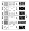
- FIG. 3 provides an overview of an implementation of Peano curves for stretchable electrodes with fractal designs.
- Panel (a) provides an illustration of three iterations of a two-dimensional Peano curve. Nine versions of the (N ⁇ 1)th curve (dotted red box) connect together with the solid red lines to construct the Nth curve.
- Panel (b) depicts arc sections replace the sharp bends to enhance the mechanics.
- Panel (c) provides an image of metal wires with Peano layouts, with an overall geometry that spell out the characters in “ILLINOIS”, mounted on skin. Here, each letter consists of a series of first and second order Peano curves.
- the “half-and-half” Peano layout which contains unit cells with alternating orientations, balances the maximum strain supported along the x- and y-axis at 16% and 13%, respectively. Such properties are well suited for devices that stretch along both axes. Adjustments to the total unit cell size can enhance the mechanics of these structures ( FIG. 20 ).
- the third order half-and-half layouts yield stretchabilities along the x- and y-axis of 32% and 28%, respectively ( FIG. 9 ).
- FIG. 20 is a diagrammatic representation of FIG. 20 .
- Electrochemical properties of the battery electrodes without and with 300% uniaxial strain appear in FIG. 23A .
- the results show two well defined plateaus at around 2.35 V corresponding to potentials of Co 3+ / 4+ and Ti 4+ / 3+ redox couples.
- the thickness of the LiCoO 2 (specific capacity 145 mAh/g) at each unit is ⁇ 120 ⁇ m, corresponding to a mass of ⁇ 95 mg, and thus areal capacity density of 1.1 mAh/cm 2 at a charge/discharge rate of C/2.
- the mass of Li 4 Ti 5 O 12 (specific capacity 160 mAh/g) is ⁇ 90 mg, which corresponds to 5%-10% more anode capacity than cathode.
- FIG. 24A shows the distributions of maximum principal strains in a large Ecoflex substrate with a diode mounted in its center, for stretching to 30%.
- FIG. 40B illustrates the distribution of the substrate normal strain at the diode/substrate interface.
- the normal interface strain in this case is negative, corresponding to compressive strain at the interface. This outcome, which is consistent with theoretical predictions based on energy release rates at an interface crack, minimizes the propensity for delamination.
- This section focuses on a geometrically simple self-similar interconnect in a rectangular configuration (as shown in FIG. 45 b ), to illustrate its structure, flexibility and stretchability.
- the rectangular interconnect is a variant of the traditional serpentine interconnect (top panel of FIG. 45 c ), and is convenient for constructing self-similar structures because of its simple geometry.
- the key is to establish the relation between the flexibility of neighboring orders, i.e., the recursion formula.
- the 1 st order (original) rectangular interconnect consists of two sets of straight wires that are perpendicular to each other and connected in series, as shown in the black box of FIG. 45 b .
- the 2 nd order rectangular interconnect shown in the blue box of FIG. 45 b , is created by reducing the scale of the 1 st order interconnect, rotating the structure by 90°, and then connecting multiple copies of it in a fashion that reproduces the layout of original geometry.
- the wide blue line in FIG. 45 b represents the 2 nd order geometry that is similar to the 1 st order rectangular geometry.
- T out ⁇ - ⁇ of ⁇ - ⁇ plane ( 2 ) ⁇ ( m , ⁇ ) ⁇ T out ⁇ - ⁇ of ⁇ - ⁇ plane , 11 ( 2 ) Sym - m 2 ⁇ ( p - 1 - v 4 ⁇ ⁇ ⁇ ⁇ ⁇ ) m ⁇ ( p - 1 - v 4 ⁇ ⁇ ⁇ ⁇ ⁇ ) 0 0 ⁇ m ⁇ ( 1 + v 2 ⁇ p + 1 - v 4 ⁇ ⁇ ⁇ ⁇ ) ⁇ , ( 4 ⁇ ⁇ b )
- T out-of-plane,11 (2) is given in Appendix.
Abstract
Description
where E is Young's modulus, L0 is the equilibrium length, ΔL is the length change under the applied stress, F is the force applied, and A is the area over which the force is applied. Young's modulus may also be expressed in terms of Lame constants via the equation:
where λ and μ are Lame constants. High Young's modulus (or “high modulus”) and low Young's modulus (or “low modulus”) are relative descriptors of the magnitude of Young's modulus in a given material, layer or device. In some embodiments, a high Young's modulus is larger than a low Young's modulus, preferably about 10 times larger for some applications, more preferably about 100 times larger for other applications, and even more preferably about 1000 times larger for yet other applications. In an embodiment, a low modulus layer has a Young's modulus less than 100 MPa, optionally less than 10 MPa, and optionally a Young's modulus selected from the range of 0.1 MPa to 50 MPa. In an embodiment, a high modulus layer has a Young's modulus greater than 100 MPa, optionally greater than 10 GPa, and optionally a Young's modulus selected from the range of 1 GPa to 100 GPa.
Rdevice is the measured resistance of the device from the four point measurement and T0 is a constant reference temperature set before the start of the experiment.
where dV/dT is from the temperature calibration. The precision of the fractal temperature sensor is 0.022° C. Mounting a device on a forearm and recording the temperature simultaneously with the sensor and an IR camera illustrates applicability to measurements on the skin.
Here U0 is the charging source of 3 volts voltage. L and R are the associated inductance and the resistance of the circuit. U(t) is the time dependent readout of the voltmeter and I(t) is the time dependent readout of an ammeter.
| #include<iostream.h> |
| #include<stdio.h> |
| #include<stdlib.h> |
| #include<math.h> |
| #include<time.h> |
| #define tim 3500 |
| #define start 265 |
| float curre[tim]; |
| float nihe[tim]; |
| float test[tim]; |
| float voll[tim]; |
| FILE *fp; |
| int main( ) |
| { |
| int i,j,k; |
| fp=fopen(“Cur.txt”,“r”); |
| for(i=0;i<tim;i++) |
| { |
| fscanf(fp,“%f”,&curre[i]); |
| curre[i]=-curre[i]; |
| cout<<curre[i]<<endl; |
| } |
| fclose(fp); |
| fp=fopen(“Vol.txt”,“r”); |
| for(i=0;i<tim;i++) |
| { |
| fscanf(fp,“%f”,&voll[i]); |
| cout<<voll[i]<<endl; |
| } |
| fclose(fp); |
| double coef1; |
| double coef2; |
| coef2=curre[1]/(voll[1]-voll[0]); |
| cout<<coef2<<endl; |
| test[0]=curre[0]; |
| test[start]=curre[start]; |
| double coef1th; |
| double maxh=1000000000; |
| double coef2th; |
| for(coef2=0;coef2<0.04; coef2=coef2+0.0001) |
| { |
| cout<<coef2<<endl; |
| for(coef1=0.94; coef1<=0.96; coef1=coef1+0.0001) |
| { |
| // cout<<coef1<<endl; |
| for(i=start+1;i<tim;i++) |
| { |
| test [i]=coef1*test [i-1]+(3- |
| (voll [i]+voll[i-1])*0.5)*coef2; |
| } |
| double poi=0; |
| for(i=start;i<tim;i++) |
| { |
| poi+=(test[i]-curre[i])*(test[i]-curre[i]); |
| } |
| if(poi<maxh) |
| { |
| coef1th=coef1; |
| coef2th=coef2; |
| maxh=poi; |
| for(int j=0;j<tim;j++) |
| { |
| nihe[j]=test[j]; |
| } |
| } |
| } |
| } |
| cout<<coef1th<<endl; |
| cout<<coef2th<<endl; |
| cout<<maxh<<endl; |
| fp=fopen(“nihe.txt”,“w”); |
| for(i=0;i<tim;i++) |
| { |
| fprintf(fp, “%f”, -nihe[i]); |
| fprintf(fp, “\n”); |
| } |
| fclose(fp); |
| fp=fopen(“canshu.txt”,“w”); |
| fprintf(fp, “%f”, coef1th); |
| fprintf(fp, “\n”); |
| fprintf(fp, “%f”, coef2th); |
| fprintf(fp, “\n”); |
| fclose(fp); |
| return(1); |
| } |
- Rogers, J. A., Someya, T. & Huang, Y. G. Materials and Mechanics for Stretchable Electronics. Science 327, 1603-1607, doi:10.1126/science.1182383 (2010).
- Wagner, S. & Bauer, S. Materials for stretchable electronics. MRS Bull. 37, 207-217, doi:10.1557/mrs.2012.37 (2012).
- Kim, D. H., Ghaffari, R., Lu, N. S. & Rogers, J. A. in Annual Review of Biomedical Engineering,
Vol 14 Vol. 14 Annual Review of Biomedical Engineering (ed M. L. Yarmush) 113-128 (Annual Reviews, 2012). - Tian, B. Z. et al. Macroporous nanowire nanoelectronic scaffolds for synthetic tissues. Nat. Mater. 11, 986-994, doi:10.1038/nmat3404 (2012).
- Takei, K. et al. Nanowire active-matrix circuitry for low-voltage macroscale artificial skin. Nat. Mater. 9, 821-826, doi:10.1038/nmat2835 (2010).
- Ramuz, M., Tee, B. C. K., Tok, J. B. H. & Bao, Z. Transparent, Optical, Pressure-Sensitive Artificial Skin for Large-Area Stretchable Electronics.
Advanced Materials 24, 3223-3227, doi:10.1002/adma.201200523 (2012). - Sekitani, T. et al. A rubberlike stretchable active matrix using elastic conductors.
Science 321, 1468-1472, doi:10.1126/science.1160309 (2008). - Ahn, B. Y. et al. Omnidirectional Printing of Flexible, Stretchable, and Spanning Silver Microelectrodes. Science 323, 1590-1593, doi:10.1126/science.1168375 (2009).
- Wu, H. et al. A transparent electrode based on a metal nanotrough network. Nat. Nanotechnol. 8, 421-425, doi:10.1038/nnano.2013.84 (2013).
- Sekitani, T. et al. Stretchable active-matrix organic light-emitting diode display using printable elastic conductors. Nat. Mater. 8, 494-499, doi:10.1038/nmat2459 (2009).
- Robinson, A. P., Minev, I., Graz, I. M. & Lacour, S. P. Microstructured Silicone Substrate for Printable and Stretchable Metallic Films.
Langmuir 27, 4279-4284, doi:10.1021/la103213n (2011). - Gray, D. S., Tien, J. & Chen, C. S. High-Conductivity Elastomeric Electronics.
Advanced Materials 16, 393-397, doi:10.1002/adma.200306107 (2004). - Brosteaux, D., Axisa, F., Gonzalez, M. & Vanfleteren, J. Design and fabrication of elastic interconnections for stretchable electronic circuits. IEEE Electron Device Lett. 28, 552-554, doi:10.1109/led.2007.897887 (2007).
- Vanfleteren, J. et al. Printed circuit board technology inspired stretchable circuits. MRS Bull. 37, 254-260, doi:10.1557/mrs.2012.48 (2012).
- Kim, D. H., Xiao, J. L., Song, J. Z., Huang, Y. G. & Rogers, J. A. Stretchable, Curvilinear Electronics Based on Inorganic Materials.
Advanced Materials 22, 2108-2124, doi:10.1002/adma.200902927 (2010). - Chen, Z. & Mecholsky, J. J. CONTROL OF STRENGTH AND TOUGHNESS OF CERAMIC-METAL LAMINATES USING INTERFACE DESIGN. Journal of
Materials Research 8, 2362-2369, doi:10.1557/jmr.1993.2362 (1993). - Connor, M. T., Roy, S., Ezquerra, T. A. & Calleja, F. J. B. Broadband ac conductivity of conductor-polymer composites. Physical Review B 57, 2286-2294, doi:10.1103/PhysRevB.57.2286 (1998).
- Hajji, P., David, L., Gerard, J. F., Pascault, J. P. & Vigier, G. Synthesis, structure, and morphology of polymer-silica hybrid nanocomposites based on hydroxyethyl methacrylate. Journal of Polymer Science Part B-
Polymer Physics 37, 3172-3187, doi:10.1002/(sici)1099-0488(19991115)37:22<3172::aid-polb2>3.0.co; 2-r (1999). - Kim, Y. et al. Stretchable nanoparticle conductors with self-organized conductive pathways.
Nature 500, 59-U77, doi:10.1038/nature12401 (2013). - Zhang, M. Q., Lu, Z. P. & Friedrich, K. On the wear debris of polyetheretherketone: Fractal dimensions in relation to wear mechanisms.
Tribology International 30, 87-102, doi:10.1016/0301-679x(96)00027-8 (1997). - Goldberger, A. L. & West, B. J. FRACTALS IN PHYSIOLOGY AND MEDICINE. Yale Journal of Biology and
Medicine 60, 4214 (1987). - Masters, B. R. Fractal analysis of the vascular tree in the human retina. Annual Review of
Biomedical Engineering 6, 427-452, doi:10.1146/annurev.bioeng.6.040803.140100 (2004). - Kim, D. H. et al. Epidermal Electronics. Science 333, 838-843, doi:10.1126/science.1206157 (2011).
- Sagan, H. Space-filling curves. (Springer-Verlag, 1994).
- Chasiotis, I. et al. Strain rate effects on the mechanical behavior of nanocrystalline Au films. Thin Solid Films 515, 3183-3189, doi:10.1016/j.tsf.2006.01.033 (2007).
- Lu, N. S., Wang, X., Suo, Z. G. & Vlassak, J. Metal films on polymer substrates stretched beyond 50%.
Applied Physics Letters 91, 3, doi:10.1063/1.2817234 (2007). - Espinosa, H. D., Prorok, B. C. & Peng, B. Plasticity size effects in free-standing submicron polycrystalline FCC films subjected to pure tension. Journal of the Mechanics and Physics of Solids 52, 667-689, doi:10.1016/j.jmps.2003.07.001 (2004).
- Chasiotis, I. & Knauss, W. G. A new microtensile tester for the study of MEMS materials with the aid of atomic force microscopy. Experimental Mechanics 42, 51-57, doi:10.1177/0018512002042001789 (2002).
- Jiang, H. et al. Finite deformation mechanics in buckled thin films on compliant supports. Proceedings of the National Academy of Sciences of the United States of
America 104, 15607-15612, doi:10.1073/pnas.0702927104 (2007). - Song, J. et al. Buckling of a stiff thin film on a compliant substrate in large deformation. International Journal of Solids and Structures 45, 3107-3121, doi:10.1016/j.ijsolstr.2008.01.023 (2008).
- Sato, K., Yoshioka, T., Ando, T., Shikida, M. & Kawabata, T. Tensile testing of silicon film having different crystallographic orientations carried out on a silicon chip. Sensors and
Actuators a -Physical 70, 148-152, doi:10.1016/s0924-4247(98)00125-3 (1998). - Jeong, J.-W. et al. Materials and Optimized Designs for Human-Machine Interfaces Via Epidermal Electronics. Advanced Materials, doi:10.1002/adma.201301921 (2013).
- Yeo, W. H. et al. Multifunctional Epidermal Electronics Printed Directly Onto the Skin.
Advanced Materials 25, 2773-2778, doi:10.1002/adma.201204426 (2013). - Fairbanks, M. S., McCarthy, D. N., Scott, S. A., Brown, S. A. & Taylor, R. P. Fractal electronic devices: simulation and implementation.
Nanotechnology 22, doi:10.1088/0957-4484/22/36/365304 (2011). - Golestanirad, L. et al. Analysis of fractal electrodes for efficient neural stimulation. Frontiers in
neuroengineering - Taylor, R. Vision of beauty.
Physics World 24, 22-27 (2011). - Webb, R. C. et al. Ultrathin conformal devices for precise and continuous thermal characterization of human skin.
Nat Mater 12, 938-944, doi:10.1038/nmat3755 - http://www.nature.com/nmat/journal/v12/n10/abs/nmat3755.html#supplementary-information (2013).
- Cohen, N. Fractal Antennas:
Part 1. Communications Quarterly, 7-22 (1995). - Gianvittorio, J. P. & Rahmat-Samii, Y. Fractal antennas: A novel antenna miniaturization technique, and applications. Ieee Antennas and
Propagation Magazine 44, 20-36, doi:10.1109/74.997888 (2002). - Puente, C., Romeu, J., Pous, R., Ramis, J. & Hijazo, A. Small but long Koch fractal monopole. Electronics Letters 34, 9-10, doi:10.1049/el:19980114 (1998).
- Pelrine, R., Kornbluh, R., Pei, Q. B. & Joseph, J. High-speed electrically actuated elastomers with strain greater than 100%. Science 287, 836-839 (2000).
- Wagner, S. et al. Electronic skin: architecture and components. Physica E Low
Dimens Syst Nanostruct 25, 326-334 (2004). - Khang, D. Y., Jiang, H. Q., Huang, Y. & Rogers, J. A. A stretchable form of single-crystal silicon for high-performance electronics on rubber substrates. Science 311, 208-212 (2006).
- Sekitani, T. et al. A rubberlike stretchable active matrix using elastic conductors.
Science 321, 1468-1472 (2008). - Sekitani, T. & Someya, T. Stretchable organic integrated circuits for large-area electronic skin surfaces.
MRS Bulletin 37, 236-245 (2012). - Suo, Z. G. Mechanics of stretchable electronics and soft machines.
MRS Bulletin 37, 218-225 (2012). - Yoon, J. et al. Ultrathin silicon solar microcells for semitransparent, mechanically flexible and microconcentrator module designs. Nature Mater. 7, 907-915 (2008).
- Kim, D. H. et al. Epidermal Electronics. Science 333, 838-843 (2011).
- Mannsfeld, S. C. B. et al. Highly sensitive flexible pressure sensors with microstructured rubber dielectric layers. Nature Mater. 9, 859-864 (2010).
- Takei, K. et al. Nanowire active-matrix circuitry for low-voltage macroscale artificial skin. Nature Mater. 9, 821-826 (2010).
- Someya, T. et al. A large-area, flexible pressure sensor matrix with organic field-effect transistors for artificial skin applications. Proc. Natl. Acad. Sci. U.S.A. 101, 9966-9970 (2004).
- Kim, D. H. et al. Materials for multifunctional balloon catheters with capabilities in cardiac electrophysiological mapping and ablation therapy. Nature Mater. 10, 316-323 (2011).
- Ko, H. C. et al. A hemispherical electronic eye camera based on compressible silicon optoelectronics. Nature 454, 748-753 (2008).
- Nishide, H. & Oyaizu, K. Toward flexible batteries. Science 319, 737-738 (2008).
- Pushparaj, V. L. et al. Flexible energy storage devices based on nanocomposite paper. Proc. Natl. Acad. Sci. U.S.A. 104, 13574-13577 (2007).
- Scrosati, B. Nanomaterials—Paper powers battery breakthrough. Nature Nanotechnol. 2, 598-599 (2007).
- Hu, L. B. et al. Highly conductive paper for energy-storage devices. Proc. Natl. Acad. Sci. U.S.A. 106, 21490-21494 (2009).
- Hu, L., Wu, H., La Mantia, F., Yang, Y. & Cui, Y. Thin, Flexible Secondary Li-Ion Paper Batteries.
ACS Nano 4, 5843-5848 (2010). - Yu, C. J., Masarapu, C., Rong, J. P., Wei, B. Q. & Jiang, H. Q. Stretchable Supercapacitors Based on Buckled Single-Walled Carbon Nanotube Macrofilms. Adv. Mater. 21, 4793-4797 (2009).
- Hu, L. B. et al. Stretchable, Porous, and Conductive Energy Textiles. Nano Lett. 10, 708-714 (2010).
- Kaltenbrunner, M., Kettlgruber, G., Siket, C., Schwodiauer, R. & Bauer, S. Arrays of Ultracompliant Electrochemical Dry Gel Cells for Stretchable Electronics. Adv. Mater. 22, 2065-2067 (2010).
- Gaikwad, A. M. et al. Highly Stretchable Alkaline Batteries Based on an Embedded Conductive Fabric. Adv. Mater. 24, 5071-5076 (2012).
- Tarascon, J. M. & Armand, M. Issues and challenges facing rechargeable lithium batteries. Nature 414, 359-367 (2001).
- Scrosati, B. & Garche, J. Lithium batteries: Status, prospects and future. J. Power Sources 195, 2419-2430 (2010).
- Thanawala, S. K. & Chaudhury, M. K. Surface modification of silicone elastomer using perfluorinated ether.
Langmuir 16, 1256-1260 (2000). - Lee, J. et al. Stretchable GaAs Photovoltaics with Designs That Enable High Areal Coverage. Adv. Mater. 23, 986-991 (2011).
- Lee, J. et al. Stretchable Semiconductor Technologies with High Areal Coverages and Strain-Limiting Behavior: Demonstration in High-Efficiency Dual-Junction GaInP/GaAs Photovoltaics. Small 8, 1851-1856 (2012).
- Krieger, K. Extreme mechanics: Buckling down. Nature 488, 146-147 (2012).
- Yoshima, K., Munakata, H. & Kanamura, K. Fabrication of micro lithium-ion battery with 3D anode and 3D cathode by using polymer wall. J. Power Sources 208, 404-408 (2012).
- Ferg, E., Gummow, R. J., Dekock, A. & Thackeray, M. M. Spinel Anodes for Lithium-Ion Batteries. J. Electrochem. Soc. 141, L147-L150 (1994).
- Owen, J. R. Rechargeable lithium batteries. Chem. Soc. Rev. 26, 259-267 (1997).
- Gowda, S. R. et al. Conformal Coating of Thin Polymer Electrolyte Layer on Nanostructured Electrode Materials for Three-Dimensional Battery Applications. Nano Lett. 11, 101-106 (2011).
- Sun, Y. G., Choi, W. M., Jiang, H. Q., Huang, Y. G. Y. & Rogers, J. A. Controlled buckling of semiconductor nanoribbons for stretchable electronics. Nature Nanotechnol. 1, 201-207 (2006).
- Ouyang, M., Yuan, C., Muisener, R. J., Boulares, A. & Koberstein, J. T. Conversion of some siloxane polymers to silicon oxide by UV/ozone photochemical processes. Chem. Mater. 12, 1591-1596 (2000).
- Datasheet for BAT 62-02LS E6327 on www.digikey.com.
h (i) =ηl (i). (1)
In addition, the height of ith order geometry equals to the distance between two ends of (i−1)th order geometry, that is
h (i)=2ml (i-1)(i=2 . . . n). (2)
Equations (1) and (2) give the length and height at any order in terms of l(n), η and m, as
l (i)=(η/2m)n-i l (n) ,h (i)=η(η/2m)n-i l (n),(i=1 . . . n). (3)
This indicates that the geometry of an arbitrary self-similar rectangular interconnect is characterized by one base length (l(n)) and three non-dimensional parameters, namely the self-similar order (n), the height/spacing ratio (η) and number (m) of unit cell. It should be mentioned that, for n≧3, there is an additional constraint on the height/spacing ratio η because of the following relation, which can be observed from the geometry of 3rd order rectangular interconnect shown in
l (i)=(2m h+1)l (i-2)(i=3 . . . n), (4)
where mh is the number of full unit cells in the structure represented by the horizontal part of the ith order geometry (i=3 . . . n). Equations (3) and (4) give the constraint on the height/spacing ratio η for n≧3
i.e., the height/spacing ratio can only take some discrete values for n≧3.
2.2. Flexibility of 1st Order Rectangular Interconnects
where W(1)=(N, Q, M)T(1)(N, Q, M)T/2 is a quadratic function of N, Q, and M for linear elastic behavior of the interconnect; and T(1) is the symmetric flexibility matrix of the 1st order interconnect and is to be determined. The strain energy also equals the sum of strain energy W(0) in all 0th order interconnects (Parts I to V), i.e.
where Wk I to Wk V represent the strain energy of each component in the kth unit cell. For the 0th order structure, i.e. a straight wire with length l and bending stiffness El, the beam theory gives the flexibility matrix as [34]
Here the membrane energy is neglected. The free body diagram of the kth unit cell of the 1st order interconnect (
Substitution of Eq. (9) into Eq. (7) gives the recursive formula between the flexibility matrices of 1st and 0th order interconnects as
Substitution of T(0) in Eq. (8) into the above equation gives a simple expression of the flexibility of 1st order interconnect in terms of the number of unit cells m, height/spacing ratio η and l(1),
where
For the 0th order structure, i.e., a straight wire of length λ, the non-dimensional flexibility matrix is defined as (u/λ, v/λ,θ)T=(λ/EI)
2.3. Flexibility of 2nd Order Rectangular Interconnect
where
is the strain energy in Part II (1st order structure, m unit cell) with
being the normalized DII in Eq. (10) (with l(1) and h(1) replaced by l(2) and h(2), respectively);
are the strain energy in Parts IV and V [0th order structure, length λ=l(2)] with
being the normalized DIV and DV in Eq. (10) [with l(1) and h(1) replaced by l(2) and h(2), respectively];
are the strain energy in Parts I and III (1st order structure, m/2 unit cell) with
being the normalized DI and DIII in Eq. (10) [with l(1) and h(1) replaced by l(2) and h(2), respectively].
results from the identity
where f=η2+η+1.
2.4. Flexibility of Higher Order Rectangular Interconnect
3.2. Generalized Self-Similar Serpentine Interconnects
where g=η(1)−1.
where p=η(2)[2η(1)+π−2]+2.
since
4.1. Generalized Self-Similar Rectangular Interconnects
For higher order structures with n≧2, the maximum strain can be well approximated by
Based on the yield criterion ∈max=∈yield, where ∈yield is the yield strain of the interconnect material (e.g., 0.3% for copper [35]), the stretchability of the generalized self-similar rectangular interconnect is obtained as
It reaches the maximum at φ=tan−1 (−N/Q), and the maximum strain is given by
The stretchability of 1st order serpentine interconnect is then obtained as [via Eq. (33)]
The normalized stretchability ∈stretchability w/[∈yieldl(1)] depends only on the height/spacing ratio η(1) and number of unit cell m(1). It increases with both η(1) and m(1), as shown in
for m(1)→∞ (also shown in
∈stretchability system=∈stretchability interconnect(1−√{square root over (f)}), (40)
where f denotes the surface filling ratio. For ˜50% surface filling ratio of active devices, the ˜100% stretchability of the interconnect translates to ˜30% stretchability of the system, which is low for some biomedical applications of stretchable electronics (to skin, heart, or elbow). The analytic models in
- [1] Lacour S P, Jones J, Wagner S, Li T, and Suo Z G. Proc IEEE 2005; 93:1459.
- [2] Lacour S P, Wagner S, Huang Z Y, and Suo Z. Appl Phys Lett 2003; 82:2404.
- [3] Lacour S P, Wagner S, Narayan R J, Li T, and Suo Z G. J Appl Phys 2006; 100: 014913.
- [4] Khang D Y, Jiang H Q, Huang Y, and Rogers J A. Science 2006; 311:208.
- [5] Kim D H, Ahn J H, Choi W M, Kim H S, Kim T H, Song J Z, Huang Y G Y, Liu Z J, Lu C, and Rogers
J A. Science 2008; 320:507. - [6] Sekitani T, Noguchi Y, Hata K, Fukushima T, Aida T, and
Someya T. Science 2008; 321:1468. - [7] Sekitani T, Nakajima H, Maeda H, Fukushima T, Aida T, Hata K, and Someya T. Nat Mater 2009; 8:494.
- [8] Kim D H, Lu N S, Ma R, Kim Y S, Kim R H, Wang S D, Wu J, Won S M, Tao H, Islam A, Yu K J, Kim T I, Chowdhury R, Ying M, Xu L Z, Li M, Chung H J, Keum H, McCormick M, Liu P, Zhang Y W, Omenetto F G, Huang Y G, Coleman T, and Rogers J A. Science 2011; 333:838.
- [9] Song Y M, Xie Y Z, Malyarchuk V, Xiao J L, Jung I, Choi K J, Liu Z J, Park H, Lu C F, Kim R H, Li R, Crozier K B, Huang Y G, and Rogers J A. Nature 2013; 497:95.
- [10] Duan Y Q, Huang Y A, and Yin Z P. Thin Solid Films 2013; 544:152.
- [11] Yoon J, Baca A J, Park S I, Elvikis P, Geddes J B, Li L F, Kim R H, Xiao J L, Wang S D, Kim T H, Motala M J, Ahn B Y, Duoss E B, Lewis J A, Nuzzo R G, Ferreira P M, Huang Y G, Rockett A, and Rogers J
A. Nat Mater 2008; 7:907. - [12] Ko H C, Stoykovich M P, Song J Z, Malyarchuk V, Choi W M, Yu C J, Geddes J B, Xiao J L, Wang S D, Huang Y G, and Rogers
J A. Nature 2008; 454:748. - [13] Wagner S, Lacour S P, Jones J, Hsu P H I, Sturm J C, Li T, and Suo Z G. Physica E 2004; 25:326.
- [14] Someya T, Sekitani T, Iba S, Kato Y, Kawaguchi H, and Sakurai T. P Natl Acad Sci USA 2004; 101:9966.
- [15] Mannsfeld S C B, Tee B C K, Stoltenberg R M, Chen C, Barman S, Muir B V O, Sokolov A N, Reese C, and Bao Z N. Nat Mater 2010; 9:859.
- [16] Saeidpourazar R, Li R, Li Y H, Sangid M D, Lu C F, Huang Y G, Rogers J A, and Ferreira P M. J Microelectromech Syst 2012; 21:1049.
- [17] Kim D H, Song J Z, Choi W M, Kim H S, Kim R H, Liu Z J, Huang Y Y, Hwang K C, Zhang Y W, and Rogers J A. P Natl
Acad Sci USA 2008; 105:18675. - [18] Lee J, Wu J A, Shi M X, Yoon J, Park S I, Li M, Liu Z J, Huang Y G, and Rogers J A. Adv Mater 2011; 23:986.
- [19] Xu S, Zhang Y H, Cho J, Lee J, Huang X, Jia L, Fan J A, Su Y W, Su J, Zhang H G, Cheng H Y, Lu B W, Yu C J, Chuang C, Kim T I, Song T, Shigeta K, Kang S, Dagdeviren C, Petrov I, Braun P V, Huang Y, Paik U, and Rogers J A. Nat Commun 2013; 4:1543.
- [20] Kim R H, Tao H, Kim T I, Zhang Y H, Kim S, Panilaitis B, Yang M M, Kim D H, Jung Y H, Kim B H, Li Y H, Huang Y G, Omenetto F G, and Rogers J A. Small 2012; 8:2812.
- [21] Jones J, Lacour S P, Wagner S, and Suo Z G. J Vac Sci Technol A 2004; 22:1723.
- [22] Gonzalez M, Axisa F, Bossuyt F, Hsu Y Y, Vandevelde B, and Vanfleteren J. Circuit World 2009; 35:22.
- [23] Gonzalez M, Axisa F, Bulcke M V, Brosteaux D, Vandevelde B, and Vanfleteren
J. Microelectron Reliab 2008; 48:825. - [24] van der Sluis O, Hsu Y Y, Timmermans P H M, Gonzalez M, and Hoefnagels J P M. J Phys D-Appl Phys 2011; 44:034008.
- [25] Hsu Y Y, Gonzalez M, Bossuyt F, Axisa F, Vanfleteren J, and De Wolf I. J Mater Res 2009; 24:3573.
- [26] Hsu Y Y, Gonzalez M, Bossuyt F, Axisa F, Vanfleteren J, and DeWolf I. J Micromech Microeng 2010; 20:075036.
- [27] Hsu Y Y, Gonzalez M, Bossuyt F, Vanfleteren J, and De Wolf I. IEEE T Electron Dev 2011; 58:2680.
- [28] Lee J, Wu J, Ryu J H, Liu Z J, Meitl M, Zhang Y W, Huang Y G, and Rogers J A. Small 2012; 8:1851.
- [29] Sun Y G, Choi W M, Jiang H Q, Huang Y G Y, and Rogers J A. Nat Nanotechnol 2006; 1:201.
- [30] Kim D H, Liu Z J, Kim Y S, Wu J, Song J Z, Kim H S, Huang Y G, Hwang K C, Zhang Y W, and Rogers J A. Small 2009; 5:2841.
- [31] Zhang Y H, Xu S, Fu H R, Lee J, Su J, Hwang K C, Rogers J A, and Huang Y. Soft Matter 2013; 9:8062.
- [32] Kim D H, Wang S D, Keum H, Ghaffari R, Kim Y S, Tao H, Panilaitis B, Li M, Kang Z, Omenetto F, Huang Y G, and Rogers J A. Small 2012; 8:3263.
- [33] Su Y W, Wu J, Fan Z C, Hwang K C, Song J Z, Huang Y G, and Rogers J A. J Mech Phys Solids 2012; 60:487.
- [34] Timoshenko S, and Gere J. Theory of Elastic Stability. New York: McGraw-Hill, 1961.
- [35] William F R, Leroy D S, and Don H M. Mechanics of Materials. New York: Jon Wiley & Sons, 1999.
- [36] Hao S J, Cui L S, Jiang D Q, Han λ D, Ren Y, Jiang J, Liu Y N, Liu Z Y, Mao S C, Wang Y D, Li Y, Ren X B, Ding X D, Wang S, Yu C, Shi X B, Du M S, Yang F, Zheng Y J, Zhang Z, Li X D, Brown D E, and Li J. Science 2013; 339:1191.
- [37] Rogers J A, Someya T, and Huang Y G. Science 2010; 327:1603.
- [38] Meitl M A, Zhu Z T, Kumar V, Lee K J, Feng X, Huang Y Y, Adesida I, Nuzzo R G, and Rogers J A. Nat Mater 2006; 5:33.
- [39] Carlson A, Bowen A M, Huang Y G, Nuzzo R G, and Rogers J A. Adv Mater 2012; 24:5284.
stretchability of the system=(1−√{square root over (filling ratio)})*(stretchability of the interconnect). (1)
Various types of interconnect technologies have been developed, typically involving planar serpentines (Jones et al., 2004; Lacour et al., 2005; Li et al., 2005; Gonzalez et al., 2008; Kim et al., 2008; Hsu et al., 2009; Kim et al., 2011 b; Kim et al., 2012c; Zhang et al., 2013c) or non-coplanar serpentines or straight bridges (Kim et al., 2008; Ko et al., 2008; Lee et al., 2011 b). In many published examples, such interconnects offer total stretchability <50% (defined by onset of cracks) and elastic stretchability <25% (defined by onset of plastic deformation), in systems that do not significantly sacrifice the filling ratio. Many applications, particularly those in optoelectronics (Ko et al., 2008; Kim et al., 2010) and energy storage systems (Lipomi et al., 2011; Xu et al., 2013), also require high filling ratios. Here, advanced interconnects are needed.
The result shows that a fractal interconnect is characterized by one base length (l(n)) and three non-dimensional parameters, namely the fractal order (n), the height/spacing ratio (η) and number (m) of unit cell.
2.2. Equivalent Flexibilities
where (EI)in-plane=Ew3t/12 and (EI)out-of-plane=Ewt3/12 are the in-plane and out-of-plane bending stiffness, respectively, and Tin-plane (n) and Tout-of-plane (n) are the normalized elastic flexibility matrices that can be obtained analytically (see Appendix). For example, the in-plane flexibility matrix for the 1st order fractal interconnect is
where Sym denotes the symmetric matrix, and g=η−1. The out-of-plane flexibility matrix for the 1st order fractal interconnect is
where v is the Poisson's ratio, and k=[4(1+v)g+(3+v)π]/4. For the 2nd order fractal interconnect, the in-plane flexibility matrix is
where p=2η2+(π−2)η+2, Tin-plane,11 (1) and Tin-plane,22 (1) are the 11 and 22 components in Eq. (4a), corresponding to the tensile and in-plane shear flexibilities, respectively. The out-of-plane flexibility matrix for the 2nd order fractal interconnect is
where Tout-of-plane,11 (2) is given in Appendix. For the higher order (n≧3) fractal interconnects, Tin-plane (n) and Tout-of-plane (n) are obtained in a recursive formula via the flexibility matrices for the (n−1)th and (n−2)th order (see Appendix).
The initially vertical 1st order fractal interconnects (blue color) become approximately horizontal (
- Cotton, D. P. J., Graz, I. M., and Lacour, S. P., 2009. A Multifunctional Capacitive Sensor for Stretchable Electronic Skins. IEEE Sensors Journal 9, 2008-2009.
- Duan, Y. Q., Huang, Y. A., Yin, Z. P., Bu, N. B., and Dong, W. T., 2014. Non-wrinkled, highly stretchable piezoelectric devices by electrohydrodynamic direct-writing. Nanoscale In Press, doi: 10.1039/C3NR06007A.
- Gao, H. J., Wang, X., Yao, H. M., Gorb, S., and Arzt, E., 2005. Mechanics of hierarchical adhesion structures of geckos. Mechanics of Materials 37, 275-285.
- Gonzalez, M., Axisa, F., Bulcke, M. V., Brosteaux, D., Vandevelde, B., and Vanfleteren, J., 2008. Design of metal interconnects for stretchable electronic circuits. Microelectronics Reliability 48, 825-832.
- Graudejus, O., Morrison, B., Goletiani, C., Yu, Z., and Wagner, S., 2012. Encapsulating Elastically Stretchable Neural Interfaces: Yield, Resolution, and Recording/Stimulation of Neural Activity. Advanced
Functional Materials 22, 640-651. - Hsu, Y. Y., Gonzalez, M., Bossuyt, F., Axisa, F., Vanfleteren, J., and De Wolf, I., 2009. In situ observations on deformation behavior and stretching-induced failure of fine pitch stretchable interconnect. Journal of Materials Research 24, 3573-3582.
- Huang, Y. A., Wang, X. M., Duan, Y. Q., Bu, N. B., and Yin, Z. P., 2012. Controllable self-organization of colloid microarrays based on finite length effects of electrospun ribbons. Soft Matter 8, 8302-8311.
- Jiang, H. Q., Khang, D. Y., Fei, H. Y., Kim, H., Huang, Y. G., Xiao, J. L., and Rogers, J. A., 2008. Finite width effect of thin-films buckling on compliant substrate: Experimental and theoretical studies. Journal of the Mechanics and Physics of Solids 56, 2585-2598.
- Jiang, H. Q., Khang, D. Y., Song, J. Z., Sun, Y. G., Huang, Y. G., and Rogers, J. A., 2007. Finite deformation mechanics in buckled thin films on compliant supports. Proceedings of the National Academy of Sciences of the United States of
America 104, 15607-15612. - Jones, J., Lacour, S. P., Wagner, S., and Suo, Z. G., 2004. Stretchable wavy metal interconnects. Journal of Vacuum Science &
Technology A 22, 1723-1725. - Kaltenbrunner, M., Sekitani, T., Reeder, J., Yokota, T., Kuribara, K., Tokuhara, T., Drack, M., Schwodiauer, R., Graz, I., Bauer-Gogonea, S., Bauer, S., and Someya, T., 2013. An ultra-lightweight design for imperceptible plastic electronics. Nature 499, 458-463.
- Khang, D. Y., Jiang, H. Q., Huang, Y., and Rogers, J. A., 2006. A stretchable form of single-crystal silicon for high-performance electronics on rubber substrates. Science 311, 208-212.
- Kim, D. H., Ghaffari, R., Lu, N. S., Wang, S. D., Lee, S. P., Keum, H., D'Angelo, R., Klinker, L., Su, Y. W., Lu, C. F., Kim, Y. S., Ameen, A., Li, Y. H., Zhang, Y. H., de Graff, B., Hsu, Y. Y., Liu, Z. J., Ruskin, J., Xu, L. Z., Lu, C., Omenetto, F. G., Huang, Y. G., Mansour, M., Slepian, M. J., and Rogers, J. A., 2012a. Electronic sensor and actuator webs for large-area complex geometry cardiac mapping and therapy. Proceedings of the National Academy of Sciences of the United States of America 109, 19910-19915.
- Kim, D. H., Liu, Z. J., Kim, Y. S., Wu, J., Song, J. Z., Kim, H. S., Huang, Y. G., Hwang, K. C., Zhang, Y. W., and Rogers, J. A., 2009. Optimized Structural Designs for Stretchable Silicon Integrated Circuits. Small 5, 2841-2847.
- Kim, D. H., Lu, N. S., Ghaffari, R., Kim, Y. S., Lee, S. P., Xu, L. Z., Wu, J. A., Kim, R. H., Song, J. Z., Liu, Z. J., Viventi, J., de Graff, B., Elolampi, B., Mansour, M., Slepian, M. J., Hwang, S., Moss, J. D., Won, S. M., Huang, Y. G., Litt, B., and Rogers, J. A., 2011a. Materials for multifunctional balloon catheters with capabilities in cardiac electrophysiological mapping and ablation therapy.
Nature Materials 10, 316-323. - Kim, D. H., Lu, N. S., Ma, R., Kim, Y. S., Kim, R. H., Wang, S. D., Wu, J., Won, S. M., Tao, H., Islam, A., Yu, K. J., Kim, T. I., Chowdhury, R., Ying, M., Xu, L. Z., Li, M., Chung, H. J., Keum, H., McCormick, M., Liu, P., Zhang, Y. W., Omenetto, F. G., Huang, Y. G., Coleman, T., and Rogers, J. A., 2011 b. Epidermal Electronics. Science 333, 838-843.
- Kim, D. H., Song, J. Z., Choi, W. M., Kim, H. S., Kim, R. H., Liu, Z. J., Huang, Y. Y., Hwang, K. C., Zhang, Y. W., and Rogers, J. A., 2008. Materials and noncoplanar mesh designs for integrated circuits with linear elastic responses to extreme mechanical deformations. Proceedings of the National Academy of Sciences of the United States of America 105, 18675-18680.
- Kim, D. H., Wang, S. D., Keum, H., Ghaffari, R., Kim, Y. S., Tao, H., Panilaitis, B., Li, M., Kang, Z., Omenetto, F., Huang, Y. G., and Rogers, J. A., 2012b. Thin, Flexible Sensors and Actuators as ‘Instrumented’ Surgical Sutures for Targeted Wound Monitoring and Therapy. Small 8, 3263-3268.
- Kim, R. H., Kim, D. H., Xiao, J. L., Kim, B. H., Park, S. I., Panilaitis, B., Ghaffari, R., Yao, J. M., Li, M., Liu, Z. J., Malyarchuk, V., Kim, D. G., Le, A. P., Nuzzo, R. G., Kaplan, D. L., Omenetto, F. G., Huang, Y. G., Kang, Z., and Rogers, J. A., 2010. Waterproof AlInGaP optoelectronics on stretchable substrates with applications in biomedicine and robotics.
Nature Materials 9, 929-937. - Kim, R. H., Tao, H., Kim, T. I., Zhang, Y. H., Kim, S., Panilaitis, B., Yang, M. M., Kim, D. H., Jung, Y. H., Kim, B. H., Li, Y. H., Huang, Y. G., Omenetto, F. G., and Rogers, J. A., 2012c. Materials and Designs for Wirelessly Powered Implantable Light-Emitting Systems. Small 8, 2812-2818.
- Ko, H. C., Stoykovich, M. P., Song, J. Z., Malyarchuk, V., Choi, W. M., Yu, C. J., Geddes, J. B., Xiao, J. L., Wang, S. D., Huang, Y. G., and Rogers, J. A., 2008. A hemispherical electronic eye camera based on compressible silicon optoelectronics. Nature 454, 748-753.
- Lacour, S. P., Jones, J., Wagner, S., Li, T., and Suo, Z. G., 2005. Stretchable interconnects for elastic electronic surfaces. Proceedings of the IEEE 93, 1459-1467.
- Lacour, S. P., Wagner, S., Narayan, R. J., Li, T., and Suo, Z. G., 2006. Stiff subcircuit islands of diamondlike carbon for stretchable electronics. Journal of
Applied Physics 100, 014913. - Lee, C. H., Kim, Y. J., Hong, Y. J., Jeon, S. R., Bae, S., Hong, B. H., and Yi, G. C., 2011a. Flexible Inorganic Nanostructure Light-Emitting Diodes Fabricated on Graphene Films.
Advanced Materials 23, 4614-4619. - Lee, J., Wu, J. A., Shi, M. X., Yoon, J., Park, S. I., Li, M., Liu, Z. J., Huang, Y. G., and Rogers, J. A., 2011b. Stretchable GaAs Photovoltaics with Designs That Enable High Areal Coverage.
Advanced Materials 23, 986-991. - Li, T., Suo, Z. G., Lacour, S. P., and Wagner, S., 2005. Compliant thin film patterns of stiff materials as platforms for stretchable electronics. Journal of
Materials Research 20, 3274-3277. - Li, Y., Ortiz, C., and Boyce, M. C., 2012. Bioinspired, mechanical, deterministic fractal model for hierarchical suture joints. Physical Review E 85,
- Li, Y., Ortiz, C., and Boyce, M. C., 2013. A generalized mechanical model for suture interfaces of arbitrary geometry. Journal of the Mechanics and Physics of
Solids 61, 1144-1167. - Lipomi, D. J., Tee, B. C. K., Vosgueritchian, M., and Bao, Z. N., 2011. Stretchable Organic Solar Cells.
Advanced Materials 23, 1771-1775. - Lu, N. S., Lu, C., Yang, S. X., and Rogers, J., 2012. Highly Sensitive Skin-Mountable Strain Gauges Based Entirely on Elastomers. Advanced
Functional Materials 22, 4044-4050. - Mannsfeld, S. C. B., Tee, B. C. K., Stoltenberg, R. M., Chen, C., Barman, S., Muir, B. V. O., Sokolov, A. N., Reese, C., and Bao, Z. N., 2010. Highly sensitive flexible pressure sensors with microstructured rubber dielectric layers.
Nature Materials 9, 859-864. - Nelson, E. C., Dias, N. L., Bassett, K. P., Dunham, S. N., Verma, V., Miyake, M., Wiltzius, P., Rogers, J. A., Coleman, J. J., Li, X. L., and Braun, P. V., 2011. Epitaxial growth of three-dimensionally architectured optoelectronic devices.
Nature Materials 10, 676-681. - Rogers, J. A., Someya, T., and Huang, Y. G., 2010. Materials and Mechanics for Stretchable Electronics. Science 327, 1603-1607.
- Sagan, H. Space-filling curves. New York: Springer-Verlag, 1994.
- Schwartz, G., Tee, B. C. K., Mei, J. G., Appleton, A. L., Kim, D. H., Wang, H. L., and Bao, Z. N., 2013. Flexible polymer transistors with high pressure sensitivity for application in electronic skin and health monitoring.
Nature Communications 4, 1859. - Sekitani, T., Nakajima, H., Maeda, H., Fukushima, T., Aida, T., Hata, K., and Someya, T., 2009. Stretchable active-matrix organic light-emitting diode display using printable elastic conductors.
Nature Materials 8, 494-499. - Someya, T., Sekitani, T., Iba, S., Kato, Y., Kawaguchi, H., and Sakurai, T., 2004. A large-area, flexible pressure sensor matrix with organic field-effect transistors for artificial skin applications. Proceedings of the National Academy of Sciences of the United States of
America 101, 9966-9970. - Song, J., Huang, Y., Xiao, J., Wang, S., Hwang, K. C., Ko, H. C., Kim, D. H., Stoykovich, M. P., and Rogers, J. A., 2009. Mechanics of noncoplanar mesh design for stretchable electronic circuits. Journal of Applied Physics 105, 123516.
- Song, Y. M., Xie, Y. Z., Malyarchuk, V., Xiao, J. L., Jung, I., Choi, K. J., Liu, Z. J., Park, H., Lu, C. F., Kim, R. H., Li, R., Crozier, K. B., Huang, Y. G., and Rogers, J. A., 2013. Digital cameras with designs inspired by the arthropod eye. Nature 497, 95-99.
- Viventi, J., Kim, D. H., Moss, J. D., Kim, Y. S., Blanco, J. A., Annetta, N., Hicks, A., Xiao, J. L., Huang, Y. G., Callans, D. J., Rogers, J. A., and Litt, B., 2010. A Conformal, Bio-Interfaced Class of Silicon Electronics for Mapping Cardiac Electrophysiology.
Science Translational Medicine 2, 24ra22. - Wagner, S., Lacour, S. P., Jones, J., Hsu, P. H. I., Sturm, J. C., Li, T., and Suo, Z. G., 2004. Electronic skin: architecture and components. Physica E-Low-Dimensional Systems &
Nanostructures 25, 326-334. - Webb, R. C., Bonifas, A. P., Behnaz, A., Zhang, Y. H., Yu, K. J., Cheng, H. Y., Shi, M. X., Bian, Z. G., Liu, Z. J., Kim, Y. S., Yeo, W. H., Park, J. S., Song, J. Z., Li, Y. H., Huang, Y. G., Gorbach, A. M., and Rogers, J. A., 2013. Ultrathin conformal devices for precise and continuous thermal characterization of human skin.
Nature Materials 12, 938-944. - William, F. R., Leroy, D. S., and Don, H. M. Mechanics of Materials. New York: Jon Wiley & Sons, 1999.
- Xu, S., Zhang, Y. H., Cho, J., Lee, J., Huang, X., Jia, L., Fan, J. A., Su, Y. W., Su, J., Zhang, H. G., Cheng, H. Y., Lu, B. W., Yu, C. J., Chuang, C., Kim, T. I., Song, T., Shigeta, K., Kang, S., Dagdeviren, C., Petrov, I., Braun, P. V., Huang, Y., Paik, U., and Rogers, J. A., 2013. Stretchable batteries with self-similar serpentine interconnects and integrated wireless recharging systems.
Nature Communications 4, 1543. - Yang, S. X., and Lu, N. S., 2013. Gauge Factor and Stretchability of Silicon-on-Polymer Strain Gauges.
Sensors 13, 8577-8594. - Yao, H., and Gao, H., 2006. Mechanics of robust and releasable adhesion in biology: Bottom-up designed hierarchical structures of gecko. Journal of the Mechanics and Physics of Solids 54, 1120-1146.
- Yao, H., and Gao, H., 2007. Multi-scale cohesive laws in hierarchical materials. International Journal of Solids and
Structures 44, 8177-8193. - Ying, M., Bonifas, A. P., Lu, N. S., Su, Y. W., Li, R., Cheng, H. Y., Ameen, A., Huang, Y. G., and Rogers, J. A., 2012. Silicon nanomembranes for fingertip electronics.
Nanotechnology 23, 344004. - Yoon, J., Baca, A. J., Park, S. I., Elvikis, P., Geddes, J. B., Li, L. F., Kim, R. H., Xiao, J. L., Wang, S. D., Kim, T. H., Motala, M. J., Ahn, B. Y., Duoss, E. B., Lewis, J. A., Nuzzo, R. G., Ferreira, P. M., Huang, Y. G., Rockett, A., and Rogers, J. A., 2008. Ultrathin silicon solar microcells for semitransparent, mechanically flexible and microconcentrator module designs.
Nature Materials 7, 907-915. - Yu, Z., Graudejus, O., Tsay, C., Lacour, S. P., Wagner, S., and Morrison, B., 2009. Monitoring Hippocampus Electrical Activity In Vitro on an Elastically Deformable Microelectrode Array. Journal of
Neurotrauma 26, 1135-1145. - Zhang, Y. H., Fu, H. R., Su, Y. W., Xu, S., Cheng, H. Y., Fan, J. A., Hwang, K. C., Rogers, J. A., and Huang, Y., 2013a. Mechanics of ultra-stretchable self-similar serpentine interconnects.
Acta Materialia 61, 7816-7827. - Zhang, Y. H., Wang, S. D., Li, X. T., Fan, J. A., Xu, S., Song, Y. M., Choi, K. J., Yeo, W. H., Lee, W., Nazaar, S. N., Lu, B. W., Yin, L., Hwang, K. C., Rogers, J. A., and Huang, Y., 2013b. Experimental and Theoretical Studies of Serpentine Microstructures Bonded To Prestrained Elastomers for Stretchable Electronics. Advanced Functional Materials In Press, doi: 10.1002/adfm.201302957.
- Zhang, Y. H., Xu, S., Fu, H. R., Lee, J., Su, J., Hwang, K. C., Rogers, J. A., and Huang, Y., 2013c. Buckling in serpentine microstructures and applications in elastomer-supported ultra-stretchable electronics with high areal coverage.
Soft Matter 9, 8062-8070. - Zhang, Z., Zhang, T., Zhang, Y. W., Kim, K.-S., and Gao, H., 2012. Strain-Controlled Switching of Hierarchically Wrinkled Surfaces between Superhydrophobicity and Superhydrophilicity.
Langmuir 28, 2753-2760. - Zhang, Z., Zhang, Y.-W., and Gao, H., 2011. On optimal hierarchy of load-bearing biological materials. Proceedings of the Royal Society B-Biological Sciences 278, 519-525.
Claims (61)
Priority Applications (2)
| Application Number | Priority Date | Filing Date | Title |
|---|---|---|---|
| US14/766,333 US9613911B2 (en) | 2013-02-06 | 2014-02-05 | Self-similar and fractal design for stretchable electronics |
| US15/477,865 US10192830B2 (en) | 2013-02-06 | 2017-04-03 | Self-similar and fractal design for stretchable electronics |
Applications Claiming Priority (5)
| Application Number | Priority Date | Filing Date | Title |
|---|---|---|---|
| US201361761412P | 2013-02-06 | 2013-02-06 | |
| US13/835,284 US10497633B2 (en) | 2013-02-06 | 2013-03-15 | Stretchable electronic systems with fluid containment |
| US201461930732P | 2014-01-23 | 2014-01-23 | |
| US14/766,333 US9613911B2 (en) | 2013-02-06 | 2014-02-05 | Self-similar and fractal design for stretchable electronics |
| PCT/US2014/014932 WO2014124044A1 (en) | 2013-02-06 | 2014-02-05 | Self-similar and fractal design for stretchable electronics |
Related Parent Applications (2)
| Application Number | Title | Priority Date | Filing Date |
|---|---|---|---|
| US13/835,284 Continuation-In-Part US10497633B2 (en) | 2013-02-06 | 2013-03-15 | Stretchable electronic systems with fluid containment |
| PCT/US2014/014932 A-371-Of-International WO2014124044A1 (en) | 2013-02-06 | 2014-02-05 | Self-similar and fractal design for stretchable electronics |
Related Child Applications (1)
| Application Number | Title | Priority Date | Filing Date |
|---|---|---|---|
| US15/477,865 Continuation US10192830B2 (en) | 2013-02-06 | 2017-04-03 | Self-similar and fractal design for stretchable electronics |
Publications (2)
| Publication Number | Publication Date |
|---|---|
| US20150380355A1 US20150380355A1 (en) | 2015-12-31 |
| US9613911B2 true US9613911B2 (en) | 2017-04-04 |
Family
ID=54931343
Family Applications (2)
| Application Number | Title | Priority Date | Filing Date |
|---|---|---|---|
| US14/766,333 Active US9613911B2 (en) | 2013-02-06 | 2014-02-05 | Self-similar and fractal design for stretchable electronics |
| US15/477,865 Active US10192830B2 (en) | 2013-02-06 | 2017-04-03 | Self-similar and fractal design for stretchable electronics |
Family Applications After (1)
| Application Number | Title | Priority Date | Filing Date |
|---|---|---|---|
| US15/477,865 Active US10192830B2 (en) | 2013-02-06 | 2017-04-03 | Self-similar and fractal design for stretchable electronics |
Country Status (1)
| Country | Link |
|---|---|
| US (2) | US9613911B2 (en) |
Cited By (51)
| Publication number | Priority date | Publication date | Assignee | Title |
|---|---|---|---|---|
| US20160217885A1 (en) * | 2015-01-27 | 2016-07-28 | Electronics And Telecommunications Research Institute | Electrically conductive stretchable interconnect using twisted nature of yarn fibers and method of manufacturing the same |
| US20180033520A1 (en) * | 2015-02-20 | 2018-02-01 | National Institute Of Advanced Industrial Science And Technology | Highly stretchable wiring, and method and device for producing the same |
| US10192830B2 (en) | 2013-02-06 | 2019-01-29 | The Board Of Trustees Of The University Of Illinois | Self-similar and fractal design for stretchable electronics |
| US10204864B2 (en) | 2004-06-04 | 2019-02-12 | The Board Of Trustees Of The University Of Illinois | Stretchable form of single crystal silicon for high performance electronics on rubber substrates |
| US10288590B2 (en) | 2013-10-08 | 2019-05-14 | Smith & Nephew Plc | PH indicator device and formulation |
| US10333069B2 (en) | 2013-04-04 | 2019-06-25 | The Board Of Trustees Of The University Of Illinois | Purification of carbon nanotubes via selective heating |
| US10374072B2 (en) | 2004-06-04 | 2019-08-06 | The Board Of Trustees Of The University Of Illinois | Methods and devices for fabricating and assembling printable semiconductor elements |
| US10396173B2 (en) | 2011-12-01 | 2019-08-27 | The Board Of Trustees Of The University Of Illinois | Transient devices designed to undergo programmable transformations |
| CN110333012A (en) * | 2019-07-24 | 2019-10-15 | 电子科技大学 | A kind of Two-dimensional strain sensor and preparation method thereof that the change of resistive appearance is compound |
| US20190331740A1 (en) * | 2017-03-29 | 2019-10-31 | Amazon Technologies, Inc. | Power supply monitoring system using strain gauges |
| US10497633B2 (en) | 2013-02-06 | 2019-12-03 | The Board Of Trustees Of The University Of Illinois | Stretchable electronic systems with fluid containment |
| US10736551B2 (en) | 2014-08-11 | 2020-08-11 | The Board Of Trustees Of The University Of Illinois | Epidermal photonic systems and methods |
| US10840536B2 (en) | 2013-02-06 | 2020-11-17 | The Board Of Trustees Of The University Of Illinois | Stretchable electronic systems with containment chambers |
| WO2021021977A1 (en) | 2019-07-31 | 2021-02-04 | Med-El Elektromedizinische Geraete Gmbh | Printed tattoo electrode respiration sensor for laryngeal pacemakers |
| US10925543B2 (en) | 2015-11-11 | 2021-02-23 | The Board Of Trustees Of The University Of Illinois | Bioresorbable silicon electronics for transient implants |
| US10950912B2 (en) | 2017-06-14 | 2021-03-16 | Milwaukee Electric Tool Corporation | Arrangements for inhibiting intrusion into battery pack electrical components |
| US11029198B2 (en) | 2015-06-01 | 2021-06-08 | The Board Of Trustees Of The University Of Illinois | Alternative approach for UV sensing |
| US11064946B2 (en) | 2014-08-11 | 2021-07-20 | The Board Of Trustees Of The University Of Illinois | Devices and related methods for epidermal characterization of biofluids |
| US11076997B2 (en) | 2017-07-25 | 2021-08-03 | Smith & Nephew Plc | Restriction of sensor-monitored region for sensor-enabled wound dressings |
| US11100817B2 (en) | 2018-06-13 | 2021-08-24 | Boe Technology Group Co., Ltd. | Flexible electronic device, manufacturing method thereof and flexible display device |
| US11118965B2 (en) | 2015-06-01 | 2021-09-14 | The Board Of Trustees Of The University Of Illinois | Miniaturized electronic systems with wireless power and near-field communication capabilities |
| US11127778B2 (en) * | 2017-02-24 | 2021-09-21 | Flexucell Aps | Light emitting transducer |
| US11154201B2 (en) | 2016-04-01 | 2021-10-26 | The Board Of Trustees Of The University Of Illinois | Implantable medical devices for optogenetics |
| US11160489B2 (en) | 2015-07-02 | 2021-11-02 | The Board Of Trustees Of The University Of Illinois | Wireless optofluidic systems for programmable in vivo pharmacology and optogenetics |
| US11160458B2 (en) | 2014-08-11 | 2021-11-02 | The Board Of Trustees Of The University Of Illinois | Epidermal devices for analysis of temperature and thermal transport characteristics |
| US20220020813A1 (en) * | 2018-02-22 | 2022-01-20 | Flexucell Aps | Light emitting transducer |
| US11293793B1 (en) | 2018-04-04 | 2022-04-05 | University Of South Alabama | Blood flow measurement apparatus and method |
| US11309305B2 (en) | 2007-01-17 | 2022-04-19 | The Board Of Trustees Of The University Of Illinois | Optical systems fabricated by printing-based assembly |
| US11322473B2 (en) * | 2019-09-12 | 2022-05-03 | International Business Machines Corporation | Interconnect and tuning thereof |
| US11324424B2 (en) | 2017-03-09 | 2022-05-10 | Smith & Nephew Plc | Apparatus and method for imaging blood in a target region of tissue |
| US20220164005A1 (en) * | 2018-12-21 | 2022-05-26 | Lg Display Co., Ltd. | Stretchable Display Panel and Stretchable Display Device Including the Same |
| US20220221354A1 (en) * | 2021-01-13 | 2022-07-14 | The Regents Of The University Of Colorado, A Body Corporate | Stretchable, rehealable, recyclable and reconfigurable integrated strain sensor |
| US11561243B2 (en) | 2019-09-12 | 2023-01-24 | International Business Machines Corporation | Compliant organic substrate assembly for rigid probes |
| US11559438B2 (en) | 2017-11-15 | 2023-01-24 | Smith & Nephew Plc | Integrated sensor enabled wound monitoring and/or therapy dressings and systems |
| US11596329B2 (en) | 2016-06-17 | 2023-03-07 | The Board Of Trustees Of The University Of Illinois | Soft, wearable microfluidic systems capable of capture, storage and sensing of biofluids |
| US11596553B2 (en) | 2017-09-27 | 2023-03-07 | Smith & Nephew Plc | Ph sensing for sensor enabled negative pressure wound monitoring and therapy apparatuses |
| US11633153B2 (en) | 2017-06-23 | 2023-04-25 | Smith & Nephew Plc | Positioning of sensors for sensor enabled wound monitoring or therapy |
| US11633147B2 (en) | 2017-09-10 | 2023-04-25 | Smith & Nephew Plc | Sensor enabled wound therapy dressings and systems implementing cybersecurity |
| US11638664B2 (en) | 2017-07-25 | 2023-05-02 | Smith & Nephew Plc | Biocompatible encapsulation and component stress relief for sensor enabled negative pressure wound therapy dressings |
| US11660005B1 (en) | 2021-06-04 | 2023-05-30 | Huxley Medical, Inc. | Processing and analyzing biometric data |
| US11690570B2 (en) | 2017-03-09 | 2023-07-04 | Smith & Nephew Plc | Wound dressing, patch member and method of sensing one or more wound parameters |
| US11706874B2 (en) | 2019-08-06 | 2023-07-18 | Microsoft Technology Licensing, Llc | Electronic-circuit printing using low-cost ink |
| US11717447B2 (en) | 2016-05-13 | 2023-08-08 | Smith & Nephew Plc | Sensor enabled wound monitoring and therapy apparatus |
| US11717221B1 (en) | 2020-03-11 | 2023-08-08 | Huxley Medical, Inc. | Patch for improved biometric data capture and related processes |
| US11759144B2 (en) | 2017-09-10 | 2023-09-19 | Smith & Nephew Plc | Systems and methods for inspection of encapsulation and components in sensor equipped wound dressings |
| US11791030B2 (en) | 2017-05-15 | 2023-10-17 | Smith & Nephew Plc | Wound analysis device and method |
| US11839464B2 (en) | 2017-09-28 | 2023-12-12 | Smith & Nephew, Plc | Neurostimulation and monitoring using sensor enabled wound monitoring and therapy apparatus |
| US11883262B2 (en) | 2017-04-11 | 2024-01-30 | Smith & Nephew Plc | Component positioning and stress relief for sensor enabled wound dressings |
| US11925735B2 (en) | 2017-08-10 | 2024-03-12 | Smith & Nephew Plc | Positioning of sensors for sensor enabled wound monitoring or therapy |
| US11931165B2 (en) | 2017-09-10 | 2024-03-19 | Smith & Nephew Plc | Electrostatic discharge protection for sensors in wound therapy |
| US11944418B2 (en) | 2018-09-12 | 2024-04-02 | Smith & Nephew Plc | Device, apparatus and method of determining skin perfusion pressure |
Families Citing this family (71)
| Publication number | Priority date | Publication date | Assignee | Title |
|---|---|---|---|---|
| US8217381B2 (en) | 2004-06-04 | 2012-07-10 | The Board Of Trustees Of The University Of Illinois | Controlled buckling structures in semiconductor interconnects and nanomembranes for stretchable electronics |
| FI126174B (en) * | 2012-12-04 | 2016-07-29 | Valmet Automation Oy | Measurement of tissue paper |
| WO2014126927A1 (en) | 2013-02-13 | 2014-08-21 | The Board Of Trustees Of The University Of Illinois | Injectable and implantable cellular-scale electronic devices |
| US9517128B2 (en) * | 2013-03-08 | 2016-12-13 | The Trustees Of Princeton University | Multi-functional hybrid devices/structures using 3D printing |
| WO2014138465A1 (en) | 2013-03-08 | 2014-09-12 | The Board Of Trustees Of The University Of Illinois | Processing techniques for silicon-based transient devices |
| WO2014157030A1 (en) * | 2013-03-27 | 2014-10-02 | 株式会社村田製作所 | Wireless power-feeding device |
| EP2984912B1 (en) | 2013-04-12 | 2020-06-24 | The Board of Trustees of the University of Illionis | Transient electrochemical devices |
| US10292263B2 (en) | 2013-04-12 | 2019-05-14 | The Board Of Trustees Of The University Of Illinois | Biodegradable materials for multilayer transient printed circuit boards |
| US9643841B2 (en) * | 2013-04-17 | 2017-05-09 | Georgia Tech Research Corporation | Graphene-based plasmonic nano-antenna for terahertz band communication |
| US9788789B2 (en) * | 2013-08-30 | 2017-10-17 | Thalmic Labs Inc. | Systems, articles, and methods for stretchable printed circuit boards |
| KR101613588B1 (en) * | 2014-05-27 | 2016-04-19 | 광주과학기술원 | Electrode arrangement with 3d structure and fabrication method thereof |
| EP2991460B1 (en) * | 2014-08-29 | 2018-11-21 | Nokia Technologies OY | An apparatus and associated methods for deformable electronics |
| US10538028B2 (en) | 2014-11-17 | 2020-01-21 | The Board Of Trustees Of The University Of Illinois | Deterministic assembly of complex, three-dimensional architectures by compressive buckling |
| KR20160089168A (en) * | 2015-01-19 | 2016-07-27 | 주식회사 아모센스 | Antenna apparatus, method manufacturing thereof, and electronic apparatus having the same |
| US9443409B1 (en) * | 2015-03-23 | 2016-09-13 | Elwha Llc | Systems to monitor proximity of body portions relative to an environment |
| US10707526B2 (en) | 2015-03-27 | 2020-07-07 | New Dominion Enterprises Inc. | All-inorganic solvents for electrolytes |
| US10098225B2 (en) * | 2015-03-31 | 2018-10-09 | Industrial Technology Research Institute | Flexible electronic module and manufacturing method thereof |
| US9836631B1 (en) | 2015-04-26 | 2017-12-05 | Aic Innovations Group, Inc. | Method and apparatus for fractal identification |
| US10729912B2 (en) * | 2015-06-05 | 2020-08-04 | Gwangju Institute Of Science And Technology | Insertable photoelectric device using absorption of light penetrating skin and electronic apparatus having same photoelectric device |
| US10452143B2 (en) * | 2015-10-20 | 2019-10-22 | San Diego State University Research Foundation | Apparatus and method of implantable bidirectional wireless neural recording and stimulation |
| KR102446889B1 (en) * | 2015-12-28 | 2022-09-26 | 삼성디스플레이 주식회사 | Flexible substrate and Flexible display device including the same |
| KR101722876B1 (en) * | 2016-04-25 | 2017-04-03 | 서울대학교산학협력단 | Loop Linked Smart Morphing Actuator |
| US20170344055A1 (en) * | 2016-05-25 | 2017-11-30 | Intel Corporation | Structural brace for electronic circuit with stretchable substrate |
| US20190209028A1 (en) * | 2016-06-30 | 2019-07-11 | Intel Corporation | Devices and methods for sensing biologic function |
| US10199323B2 (en) | 2016-08-30 | 2019-02-05 | Apple Inc. | Flexible circuit substrate with temporary supports and equalized lateral expansion |
| KR20180026007A (en) * | 2016-09-01 | 2018-03-12 | 삼성디스플레이 주식회사 | Transparent electrode and manufacturing method thereof |
| JP6972523B2 (en) * | 2016-09-13 | 2021-11-24 | セイコーエプソン株式会社 | Electronics |
| US10707531B1 (en) | 2016-09-27 | 2020-07-07 | New Dominion Enterprises Inc. | All-inorganic solvents for electrolytes |
| US10786202B2 (en) * | 2016-09-28 | 2020-09-29 | International Business Machines Corporation | Quantifying grip strength and characterizing movement idioms |
| KR102646349B1 (en) * | 2016-11-15 | 2024-03-11 | 가부시끼가이샤 레조낙 | Method of manufacturing conductor boards, wiring boards and wiring boards |
| JP6770743B2 (en) * | 2016-12-20 | 2020-10-21 | 北川工業株式会社 | Pressure sensor |
| WO2018135888A1 (en) * | 2017-01-18 | 2018-07-26 | 주식회사 케이티앤지 | Aerosol generating device, method for controlling same, and charging system including same |
| KR101987235B1 (en) * | 2017-01-18 | 2019-09-30 | 주식회사 케이티앤지 | Heater of electric heating smoking apparatus |
| KR102183092B1 (en) * | 2017-01-18 | 2020-11-25 | 주식회사 케이티앤지 | Power-efficient fine particle generator |
| JP6898048B2 (en) | 2017-01-18 | 2021-07-07 | ケーティー・アンド・ジー・コーポレーション | Aerosol generator, its control method, and charging system including it |
| US11435739B2 (en) * | 2017-02-08 | 2022-09-06 | L. Samuel A Kassatly | Interface and method for controlling the operation of an autonomously travelling object |
| US10496218B2 (en) * | 2017-02-08 | 2019-12-03 | Apple Inc. | Display stack with integrated force input sensor |
| CN106821378A (en) * | 2017-03-21 | 2017-06-13 | 成都柔电云科科技有限公司 | A kind of portable muscular fatigue degree testing equipment based on electronics epidermis |
| US10535845B1 (en) * | 2017-07-14 | 2020-01-14 | Flex Ltd. | Flexible and stretchable chain battery |
| KR20190047436A (en) * | 2017-10-27 | 2019-05-08 | 서울대학교산학협력단 | Core-shell nanowire, method of forming the core-shell nanowire, and stretchable composites comprising the core-shell nanowire |
| US11154232B2 (en) | 2017-11-14 | 2021-10-26 | The Board Of Trustees Of The University Of Illinois | Mechano-acoustic sensing devices and methods |
| US10799403B2 (en) | 2017-12-28 | 2020-10-13 | Stryker Corporation | Patient transport apparatus with controlled auxiliary wheel deployment |
| EP3735733B1 (en) * | 2018-01-04 | 2024-01-17 | Tc1 Llc | Systems and methods for elastic wireless power transmission devices |
| US10687421B1 (en) | 2018-04-04 | 2020-06-16 | Flex Ltd. | Fabric with woven wire braid |
| KR102530672B1 (en) | 2018-07-20 | 2023-05-08 | 엘지디스플레이 주식회사 | Stretchable display device |
| KR102554048B1 (en) | 2018-07-20 | 2023-07-10 | 엘지디스플레이 주식회사 | Stretchable display device |
| KR102588626B1 (en) | 2018-07-27 | 2023-10-11 | 엘지디스플레이 주식회사 | Flexible printed circuit and stretchable display device comprising the same |
| US11464964B2 (en) * | 2018-08-03 | 2022-10-11 | Brown University | Neural interrogation platform |
| EP3608964B1 (en) | 2018-08-08 | 2022-05-11 | LG Display Co., Ltd. | Stretchable display device |
| CN109147584B (en) * | 2018-08-10 | 2024-02-09 | 佛山市国星光电股份有限公司 | LED display unit group and display panel |
| US10779403B2 (en) | 2018-09-20 | 2020-09-15 | Apple Inc. | Shorting pattern between pads of a camera module |
| KR20200039973A (en) | 2018-10-08 | 2020-04-17 | 엘지디스플레이 주식회사 | Stretchable display device and manufacturing method the same |
| US11202914B2 (en) * | 2018-12-21 | 2021-12-21 | Medtronic, Inc. | Passive propagation fractal antenna for intrabody transmissions |
| US10903415B2 (en) * | 2019-02-04 | 2021-01-26 | United Technologies Corporation | Large structure monitoring with a substrate-free flexible sensor system |
| CN109920334B (en) | 2019-03-27 | 2021-04-27 | 京东方科技集团股份有限公司 | Array substrate and display device |
| TWI745704B (en) * | 2019-06-21 | 2021-11-11 | 國立陽明交通大學 | Nio chip and the preparing method and use thereof |
| CN110849514B (en) * | 2019-10-15 | 2021-09-28 | 杭州电子科技大学 | High-performance rGO/CNF force electric sensor and preparation method thereof |
| EP3843067A1 (en) * | 2019-12-24 | 2021-06-30 | LG Display Co., Ltd. | Stretchable display device |
| US20210228864A1 (en) * | 2020-01-08 | 2021-07-29 | Purdue Research Foundation | Electronic devices, electrodes thereof, and methods for producing the same |
| US20210213446A1 (en) * | 2020-01-09 | 2021-07-15 | Novoheart Limited | Sample analysis device |
| KR20210102506A (en) * | 2020-02-10 | 2021-08-20 | 삼성디스플레이 주식회사 | Electronic device and method of manufacturing the electronic device |
| CN112001038B (en) * | 2020-06-24 | 2023-03-31 | 中国科学院新疆天文台 | Method for determining adjustment quantity of active main reflector antenna actuator based on panel adjustment matrix |
| CN113922081A (en) * | 2020-07-08 | 2022-01-11 | 北京小米移动软件有限公司 | Electronic device |
| RS20201065A1 (en) | 2020-09-04 | 2022-03-31 | Inst Biosens Istrazivacko Razvojni Inst Za Informacione Tehnologije Biosistema | Planar electrode for biosensors realized using repetitive fractal geometry |
| KR102455351B1 (en) | 2020-10-13 | 2022-10-18 | 한국기계연구원 | Stretchable battery |
| TWI788740B (en) * | 2020-12-09 | 2023-01-01 | 財團法人工業技術研究院 | Stretchable circuit and layout method of the stretchable circuit |
| CN112863340A (en) * | 2021-01-12 | 2021-05-28 | 武汉华星光电半导体显示技术有限公司 | Stretchable display module |
| WO2022174856A1 (en) | 2021-02-20 | 2022-08-25 | Christian-Albrechts-Universität Zu Kiel | Auxetic web structure or field structure, and use |
| CN113066929B (en) * | 2021-03-15 | 2022-08-16 | 中国科学院半导体研究所 | Fractal lumped capacitor based on mole curve and preparation method thereof |
| FR3123762A1 (en) * | 2021-06-07 | 2022-12-09 | Commissariat A L'energie Atomique Et Aux Energies Alternatives | Electrical interconnection element of at least two photovoltaic cells |
| US20230088896A1 (en) * | 2021-09-20 | 2023-03-23 | Wei-Jan Lin | Fractal structure system |
Citations (60)
| Publication number | Priority date | Publication date | Assignee | Title |
|---|---|---|---|---|
| US5171482A (en) | 1989-08-31 | 1992-12-15 | Dow Corning Toray Silicone Co., Ltd | Silicone composition which does not cause faulty conduction at electrical contacts, and method for preventing conduction faults |
| US5477067A (en) | 1987-05-27 | 1995-12-19 | Hitachi, Ltd. | Semiconductor IC device having a RAM interposed between different logic sections and by-pass signal lines extending over the RAM for mutually connecting the logic sections |
| US5663106A (en) | 1994-05-19 | 1997-09-02 | Tessera, Inc. | Method of encapsulating die and chip carrier |
| US5739463A (en) | 1994-04-11 | 1998-04-14 | Raychem Corporation | Sealed electronic packaging for environmental protection of active electronics |
| US5967986A (en) | 1997-11-25 | 1999-10-19 | Vascusense, Inc. | Endoluminal implant with fluid flow sensing capability |
| US6020219A (en) | 1994-06-16 | 2000-02-01 | Lucent Technologies Inc. | Method of packaging fragile devices with a gel medium confined by a rim member |
| US20020109219A1 (en) | 2001-02-13 | 2002-08-15 | Yang Chung Hsien | Semiconductor package with heat sink having air vent |
| US6489669B2 (en) | 2000-09-11 | 2002-12-03 | Rohm Co., Ltd. | Integrated circuit device |
| US6614108B1 (en) | 2000-10-23 | 2003-09-02 | Delphi Technologies, Inc. | Electronic package and method therefor |
| US6617683B2 (en) | 2001-09-28 | 2003-09-09 | Intel Corporation | Thermal performance in flip chip/integral heat spreader packages using low modulus thermal interface material |
| US20050253273A1 (en) * | 2003-11-05 | 2005-11-17 | California Institute Of Technology | Method for integrating pre-fabricated chip structures into functional electronic systems |
| US6993392B2 (en) | 2002-03-14 | 2006-01-31 | Duke University | Miniaturized high-density multichannel electrode array for long-term neuronal recordings |
| US20060071349A1 (en) * | 2004-10-06 | 2006-04-06 | Nobuaki Tokushige | Semiconductor device and semiconductor device unit |
| US7195733B2 (en) | 2004-04-27 | 2007-03-27 | The Board Of Trustees Of The University Of Illinois | Composite patterning devices for soft lithography |
| US20080055581A1 (en) | 2004-04-27 | 2008-03-06 | Rogers John A | Devices and methods for pattern generation by ink lithography |
| US20080157095A1 (en) | 2004-06-12 | 2008-07-03 | Samsung Electronics Co., Ltd. | Semiconductor Devices Having Single Crystalline Silicon Layers |
| US20080193855A1 (en) | 2006-10-04 | 2008-08-14 | Mcdonald Robert C | Electrolyte suitable for use in a lithium ion cell or battery |
| US7491892B2 (en) * | 2003-03-28 | 2009-02-17 | Princeton University | Stretchable and elastic interconnects |
| US7521292B2 (en) | 2004-06-04 | 2009-04-21 | The Board Of Trustees Of The University Of Illinois | Stretchable form of single crystal silicon for high performance electronics on rubber substrates |
| US7557367B2 (en) | 2004-06-04 | 2009-07-07 | The Board Of Trustees Of The University Of Illinois | Stretchable semiconductor elements and stretchable electrical circuits |
| US7705280B2 (en) | 2006-07-25 | 2010-04-27 | The Board Of Trustees Of The University Of Illinois | Multispectral plasmonic crystal sensors |
| US7704684B2 (en) | 2003-12-01 | 2010-04-27 | The Board Of Trustees Of The University Of Illinois | Methods and devices for fabricating three-dimensional nanoscale structures |
| US20100116526A1 (en) * | 2008-10-07 | 2010-05-13 | Arora William J | Extremely stretchable electronics |
| US20100157804A1 (en) | 2008-12-17 | 2010-06-24 | Embarq Holdings Company, Llc | System and method for tracking maximum throughput and sla compliance |
| US20100178722A1 (en) * | 2008-10-07 | 2010-07-15 | De Graff Bassel | Methods and applications of non-planar imaging arrays |
| WO2010086034A1 (en) * | 2009-01-30 | 2010-08-05 | Interuniversitair Microelektronica Centrum Vzw | Stretchable electronic device |
| US7799699B2 (en) | 2004-06-04 | 2010-09-21 | The Board Of Trustees Of The University Of Illinois | Printable semiconductor structures and related methods of making and assembling |
| US7932123B2 (en) | 2006-09-20 | 2011-04-26 | The Board Of Trustees Of The University Of Illinois | Release strategies for making transferable semiconductor structures, devices and device components |
| US7943491B2 (en) | 2004-06-04 | 2011-05-17 | The Board Of Trustees Of The University Of Illinois | Pattern transfer printing by kinetic control of adhesion to an elastomeric stamp |
| US7972875B2 (en) | 2007-01-17 | 2011-07-05 | The Board Of Trustees Of The University Of Illinois | Optical systems fabricated by printing-based assembly |
| US20120038027A1 (en) | 2010-08-11 | 2012-02-16 | Marcel Broekaart | Method for molecular adhesion bonding at low pressure |
| US20120051005A1 (en) * | 2009-01-30 | 2012-03-01 | Universiteit Gent | Stretchable electronic device |
| US20120121963A1 (en) | 2010-11-16 | 2012-05-17 | Samsung Electronics Co., Ltd. | Flexible battery and flexible electronic device including the same |
| US20120157804A1 (en) | 2009-12-16 | 2012-06-21 | Rogers John A | High-Speed, High-Resolution Electrophysiology In-Vivo Using Conformal Electronics |
| US20120165759A1 (en) | 2009-12-16 | 2012-06-28 | Rogers John A | Waterproof stretchable optoelectronics |
| US8217381B2 (en) | 2004-06-04 | 2012-07-10 | The Board Of Trustees Of The University Of Illinois | Controlled buckling structures in semiconductor interconnects and nanomembranes for stretchable electronics |
| US20120261551A1 (en) | 2011-01-14 | 2012-10-18 | Rogers John A | Optical component array having adjustable curvature |
| US20120320581A1 (en) | 2011-05-16 | 2012-12-20 | Rogers John A | Thermally Managed LED Arrays Assembled by Printing |
| US8367035B2 (en) | 2006-03-03 | 2013-02-05 | The Board Of Trustees Of The University Of Illinois | Methods of making spatially aligned nanotubes and nanotube arrays |
| US20130036928A1 (en) | 2011-07-14 | 2013-02-14 | John A. Rogers | Non-contact transfer printing |
| US20130041235A1 (en) | 2009-12-16 | 2013-02-14 | John A. Rogers | Flexible and Stretchable Electronic Systems for Epidermal Electronics |
| US20130140649A1 (en) | 2011-12-01 | 2013-06-06 | John A. Rogers | Transient devices designed to undergo programmable transformations |
| US8470701B2 (en) | 2008-04-03 | 2013-06-25 | Advanced Diamond Technologies, Inc. | Printable, flexible and stretchable diamond for thermal management |
| US8552299B2 (en) | 2008-03-05 | 2013-10-08 | The Board Of Trustees Of The University Of Illinois | Stretchable and foldable electronic devices |
| US8562095B2 (en) | 2010-11-01 | 2013-10-22 | The Board Of Trustees Of The University Of Illinois | High resolution sensing and control of electrohydrodynamic jet printing |
| US20130333094A1 (en) | 2012-03-30 | 2013-12-19 | The Board Of Trustees Of The University Of Illinois | Appendage Mountable Electronic Devices COnformable to Surfaces |
| US8666471B2 (en) | 2010-03-17 | 2014-03-04 | The Board Of Trustees Of The University Of Illinois | Implantable biomedical devices on bioresorbable substrates |
| US8679888B2 (en) | 2008-09-24 | 2014-03-25 | The Board Of Trustees Of The University Of Illinois | Arrays of ultrathin silicon solar microcells |
| US20140220422A1 (en) | 2013-02-06 | 2014-08-07 | The Board Of Trustees Of The University Of Illinois | Stretchable electronic systems with fluid containment |
| US20140305900A1 (en) | 2013-04-12 | 2014-10-16 | The Board Of Trustees Of The University Of Illinois | Transient electronic devices comprising inorganic or hybrid inorganic and organic substrates and encapsulates |
| US8865489B2 (en) | 2009-05-12 | 2014-10-21 | The Board Of Trustees Of The University Of Illinois | Printed assemblies of ultrathin, microscale inorganic light emitting diodes for deformable and semitransparent displays |
| US8934965B2 (en) | 2011-06-03 | 2015-01-13 | The Board Of Trustees Of The University Of Illinois | Conformable actively multiplexed high-density surface electrode array for brain interfacing |
| US8946683B2 (en) | 2008-06-16 | 2015-02-03 | The Board Of Trustees Of The University Of Illinois | Medium scale carbon nanotube thin film integrated circuits on flexible plastic substrates |
| US20150141767A1 (en) | 2013-10-02 | 2015-05-21 | The Board Of Trustees Of The University Of Illinois | Organ Mounted Electronics |
| US9057994B2 (en) | 2010-01-08 | 2015-06-16 | The Board Of Trustees Of The University Of Illinois | High resolution printing of charge |
| US9061494B2 (en) | 2007-07-19 | 2015-06-23 | The Board Of Trustees Of The University Of Illinois | High resolution electrohydrodynamic jet printing for manufacturing systems |
| US20150207012A1 (en) | 2014-01-16 | 2015-07-23 | The Board Of Trustees Of The University Of Illinois | Printing-based assembly of multi-junction, multi-terminal photovoltaic devices and related methods |
| US20150373831A1 (en) | 2013-02-06 | 2015-12-24 | Lin Jia | Stretchable electronic systems with containment chambers |
| US20150380355A1 (en) | 2013-02-06 | 2015-12-31 | John A. Rogers | Self-similar and fractal design for stretchable electronics |
| US20160005700A1 (en) | 2013-03-08 | 2016-01-07 | The Board Of Trustees Of The University Of Illinois | Processing techniques for silicon-based transient devices |
Family Cites Families (35)
| Publication number | Priority date | Publication date | Assignee | Title |
|---|---|---|---|---|
| JPS607056A (en) | 1983-06-25 | 1985-01-14 | Tomoyuki Aoki | Manufacture of flexible thin battery |
| NO911774D0 (en) | 1991-05-06 | 1991-05-06 | Sensonor As | DEVICE FOR ENCAPLING A FUNCTIONAL ORGANIZATION AND PROCEDURE FOR PRODUCING THE SAME. |
| EP0703613A3 (en) | 1994-09-26 | 1996-06-05 | Motorola Inc | Protecting electronic components in acidic and basic environments |
| JPH10125825A (en) | 1996-10-23 | 1998-05-15 | Nec Corp | Seal structure of chip device and method of sealing the same |
| DE60022096T2 (en) | 2000-01-19 | 2006-06-01 | Fractus, S.A. | ROOM FILLING MINIATURE ANTENNA |
| JP2001237351A (en) | 2000-02-22 | 2001-08-31 | Hitachi Maxell Ltd | Semiconductor device |
| US6743982B2 (en) | 2000-11-29 | 2004-06-01 | Xerox Corporation | Stretchable interconnects using stress gradient films |
| AU2002367630A1 (en) | 2002-02-12 | 2003-09-04 | Eveready Battery Company, Inc. | Flexible thin printed battery with gelled electrolyte and method of manufacturing same |
| JP4346333B2 (en) | 2003-03-26 | 2009-10-21 | 新光電気工業株式会社 | Method for manufacturing multilayer circuit board incorporating semiconductor element |
| WO2010056771A1 (en) | 2008-11-11 | 2010-05-20 | Shifamed Llc | Low profile electrode assembly |
| US8187795B2 (en) | 2008-12-09 | 2012-05-29 | The Board Of Trustees Of The University Of Illinois | Patterning methods for stretchable structures |
| US8883287B2 (en) | 2009-06-29 | 2014-11-11 | Infinite Corridor Technology, Llc | Structured material substrates for flexible, stretchable electronics |
| DE102009031568A1 (en) | 2009-06-29 | 2010-12-30 | Fraunhofer-Gesellschaft zur Förderung der angewandten Forschung e.V. | Method for producing an electronic system, method for producing a free-form surface with such a system, as well as electronic system and free-form surfaces with such a system |
| DE102010030960B4 (en) | 2010-07-06 | 2020-12-10 | Robert Bosch Gmbh | Process for manufacturing a vibration-damped component |
| DE102011003195B4 (en) | 2011-01-26 | 2019-01-10 | Robert Bosch Gmbh | Component and method for manufacturing a component |
| GB2529346A (en) | 2011-03-31 | 2016-02-17 | Plasyl Ltd | Improvements for electrical circuits |
| DE102011007058A1 (en) | 2011-04-08 | 2012-10-11 | Fraunhofer-Gesellschaft zur Förderung der angewandten Forschung e.V. | Electrical trace |
| JP6029262B2 (en) | 2011-04-26 | 2016-11-24 | 日本メクトロン株式会社 | Flexible circuit body |
| US8895864B2 (en) | 2012-03-30 | 2014-11-25 | Nokia Corporation | Deformable apparatus and method |
| WO2014126927A1 (en) | 2013-02-13 | 2014-08-21 | The Board Of Trustees Of The University Of Illinois | Injectable and implantable cellular-scale electronic devices |
| US9825229B2 (en) | 2013-04-04 | 2017-11-21 | The Board Of Trustees Of The University Of Illinois | Purification of carbon nanotubes via selective heating |
| US10292263B2 (en) | 2013-04-12 | 2019-05-14 | The Board Of Trustees Of The University Of Illinois | Biodegradable materials for multilayer transient printed circuit boards |
| US9706647B2 (en) * | 2013-05-14 | 2017-07-11 | Mc10, Inc. | Conformal electronics including nested serpentine interconnects |
| US9554465B1 (en) * | 2013-08-27 | 2017-01-24 | Flextronics Ap, Llc | Stretchable conductor design and methods of making |
| US9231327B1 (en) * | 2013-08-27 | 2016-01-05 | Flextronics Ap, Llc | Electronic circuit slidable interconnect |
| KR20170041291A (en) | 2014-08-11 | 2017-04-14 | 더 보오드 오브 트러스티스 오브 더 유니버시티 오브 일리노이즈 | Devices and related methods for epidermal characterization of biofluids |
| US10736551B2 (en) | 2014-08-11 | 2020-08-11 | The Board Of Trustees Of The University Of Illinois | Epidermal photonic systems and methods |
| KR102244435B1 (en) * | 2014-09-03 | 2021-04-26 | 삼성디스플레이 주식회사 | Flexible circuit board and electronic device including the same |
| US10538028B2 (en) | 2014-11-17 | 2020-01-21 | The Board Of Trustees Of The University Of Illinois | Deterministic assembly of complex, three-dimensional architectures by compressive buckling |
| US20170020402A1 (en) | 2015-05-04 | 2017-01-26 | The Board Of Trustees Of The University Of Illinois | Implantable and bioresorbable sensors |
| BR112017025609A2 (en) | 2015-06-01 | 2018-08-07 | The Board Of Trustees Of The University Of Illinois | miniaturized wireless electronic systems with near field communication capabilities |
| EP3304130B1 (en) | 2015-06-01 | 2021-10-06 | The Board of Trustees of the University of Illinois | Alternative approach to uv sensing |
| WO2017004531A1 (en) | 2015-07-02 | 2017-01-05 | The Board Of Trustees Of The University Of Illinois | Fully implantable soft medical devices for interfacing with biological tissue |
| US11160489B2 (en) | 2015-07-02 | 2021-11-02 | The Board Of Trustees Of The University Of Illinois | Wireless optofluidic systems for programmable in vivo pharmacology and optogenetics |
| US10925543B2 (en) | 2015-11-11 | 2021-02-23 | The Board Of Trustees Of The University Of Illinois | Bioresorbable silicon electronics for transient implants |
-
2014
- 2014-02-05 US US14/766,333 patent/US9613911B2/en active Active
-
2017
- 2017-04-03 US US15/477,865 patent/US10192830B2/en active Active
Patent Citations (89)
| Publication number | Priority date | Publication date | Assignee | Title |
|---|---|---|---|---|
| US5477067A (en) | 1987-05-27 | 1995-12-19 | Hitachi, Ltd. | Semiconductor IC device having a RAM interposed between different logic sections and by-pass signal lines extending over the RAM for mutually connecting the logic sections |
| US5171482A (en) | 1989-08-31 | 1992-12-15 | Dow Corning Toray Silicone Co., Ltd | Silicone composition which does not cause faulty conduction at electrical contacts, and method for preventing conduction faults |
| US5739463A (en) | 1994-04-11 | 1998-04-14 | Raychem Corporation | Sealed electronic packaging for environmental protection of active electronics |
| US5663106A (en) | 1994-05-19 | 1997-09-02 | Tessera, Inc. | Method of encapsulating die and chip carrier |
| US6020219A (en) | 1994-06-16 | 2000-02-01 | Lucent Technologies Inc. | Method of packaging fragile devices with a gel medium confined by a rim member |
| US5967986A (en) | 1997-11-25 | 1999-10-19 | Vascusense, Inc. | Endoluminal implant with fluid flow sensing capability |
| US6489669B2 (en) | 2000-09-11 | 2002-12-03 | Rohm Co., Ltd. | Integrated circuit device |
| US6614108B1 (en) | 2000-10-23 | 2003-09-02 | Delphi Technologies, Inc. | Electronic package and method therefor |
| US20020109219A1 (en) | 2001-02-13 | 2002-08-15 | Yang Chung Hsien | Semiconductor package with heat sink having air vent |
| US6617683B2 (en) | 2001-09-28 | 2003-09-09 | Intel Corporation | Thermal performance in flip chip/integral heat spreader packages using low modulus thermal interface material |
| US6993392B2 (en) | 2002-03-14 | 2006-01-31 | Duke University | Miniaturized high-density multichannel electrode array for long-term neuronal recordings |
| US7491892B2 (en) * | 2003-03-28 | 2009-02-17 | Princeton University | Stretchable and elastic interconnects |
| US20050253273A1 (en) * | 2003-11-05 | 2005-11-17 | California Institute Of Technology | Method for integrating pre-fabricated chip structures into functional electronic systems |
| US7704684B2 (en) | 2003-12-01 | 2010-04-27 | The Board Of Trustees Of The University Of Illinois | Methods and devices for fabricating three-dimensional nanoscale structures |
| US7195733B2 (en) | 2004-04-27 | 2007-03-27 | The Board Of Trustees Of The University Of Illinois | Composite patterning devices for soft lithography |
| US20080055581A1 (en) | 2004-04-27 | 2008-03-06 | Rogers John A | Devices and methods for pattern generation by ink lithography |
| US8754396B2 (en) | 2004-06-04 | 2014-06-17 | The Board Of Trustees Of The University Of Illinois | Stretchable form of single crystal silicon for high performance electronics on rubber substrates |
| US20150001462A1 (en) | 2004-06-04 | 2015-01-01 | The Board Of Trustees Of The University Of Illinois | Stretchable Form of Single Crystal Silicon for High Performance Electronics on Rubber Substrates |
| US7521292B2 (en) | 2004-06-04 | 2009-04-21 | The Board Of Trustees Of The University Of Illinois | Stretchable form of single crystal silicon for high performance electronics on rubber substrates |
| US7557367B2 (en) | 2004-06-04 | 2009-07-07 | The Board Of Trustees Of The University Of Illinois | Stretchable semiconductor elements and stretchable electrical circuits |
| US7622367B1 (en) | 2004-06-04 | 2009-11-24 | The Board Of Trustees Of The University Of Illinois | Methods and devices for fabricating and assembling printable semiconductor elements |
| US8729524B2 (en) | 2004-06-04 | 2014-05-20 | The Board Of Trustees Of The University Of Illinois | Controlled buckling structures in semiconductor interconnects and nanomembranes for stretchable electronics |
| US20140191236A1 (en) | 2004-06-04 | 2014-07-10 | The Board Of Trustees Of The University Of Iiiinois | Methods and Devices for Fabricating and Assembling Printable Semiconductor Elements |
| US8664699B2 (en) | 2004-06-04 | 2014-03-04 | The Board Of Trustees Of The University Of Illinois | Methods and devices for fabricating and assembling printable semiconductor elements |
| US20140374872A1 (en) | 2004-06-04 | 2014-12-25 | The Board Of Trustees Of The University Of Illinois | Controlled Buckling Structures in Semiconductor Interconnects and Nanomembranes for Stretchable Electronics |
| US8198621B2 (en) | 2004-06-04 | 2012-06-12 | The Board Of Trustees Of The University Of Illinois | Stretchable form of single crystal silicon for high performance electronics on rubber substrates |
| US8440546B2 (en) | 2004-06-04 | 2013-05-14 | The Board Of Trustees Of The University Of Illinois | Methods and devices for fabricating and assembling printable semiconductor elements |
| US7799699B2 (en) | 2004-06-04 | 2010-09-21 | The Board Of Trustees Of The University Of Illinois | Printable semiconductor structures and related methods of making and assembling |
| US8394706B2 (en) | 2004-06-04 | 2013-03-12 | The Board Of Trustees Of The University Of Illinois | Printable semiconductor structures and related methods of making and assembling |
| US7943491B2 (en) | 2004-06-04 | 2011-05-17 | The Board Of Trustees Of The University Of Illinois | Pattern transfer printing by kinetic control of adhesion to an elastomeric stamp |
| US9105555B2 (en) | 2004-06-04 | 2015-08-11 | The Board Of Trustees Of The University Of Illinois | Stretchable form of single crystal silicon for high performance electronics on rubber substrates |
| US7982296B2 (en) | 2004-06-04 | 2011-07-19 | The Board Of Trustees Of The University Of Illinois | Methods and devices for fabricating and assembling printable semiconductor elements |
| US8039847B2 (en) | 2004-06-04 | 2011-10-18 | The Board Of Trustees Of The University Of Illinois | Printable semiconductor structures and related methods of making and assembling |
| US8217381B2 (en) | 2004-06-04 | 2012-07-10 | The Board Of Trustees Of The University Of Illinois | Controlled buckling structures in semiconductor interconnects and nanomembranes for stretchable electronics |
| US20160027737A1 (en) | 2004-06-04 | 2016-01-28 | The Board Of Trustees Of The University Of Illinois | Stretchable Form of Single Crystal Silicon for High Performance Electronics on Rubber Substrates |
| US20080157095A1 (en) | 2004-06-12 | 2008-07-03 | Samsung Electronics Co., Ltd. | Semiconductor Devices Having Single Crystalline Silicon Layers |
| US20060071349A1 (en) * | 2004-10-06 | 2006-04-06 | Nobuaki Tokushige | Semiconductor device and semiconductor device unit |
| US8367035B2 (en) | 2006-03-03 | 2013-02-05 | The Board Of Trustees Of The University Of Illinois | Methods of making spatially aligned nanotubes and nanotube arrays |
| US7705280B2 (en) | 2006-07-25 | 2010-04-27 | The Board Of Trustees Of The University Of Illinois | Multispectral plasmonic crystal sensors |
| US7932123B2 (en) | 2006-09-20 | 2011-04-26 | The Board Of Trustees Of The University Of Illinois | Release strategies for making transferable semiconductor structures, devices and device components |
| US20140361409A1 (en) | 2006-09-20 | 2014-12-11 | The Board Of Trustees Of The University Of Illinois | Release Strategies for Making Transferable Semiconductor Structures, Devices and Device Components |
| US20110316120A1 (en) | 2006-09-20 | 2011-12-29 | The Board Of Trustees Of The University Of Illinois | Release Strategies for Making Transferable Semiconductor Structures, Devices and Device Components |
| US8895406B2 (en) | 2006-09-20 | 2014-11-25 | The Board Of Trustees Of The University Of Illinois | Release strategies for making transferable semiconductor structures, devices and device components |
| US20080193855A1 (en) | 2006-10-04 | 2008-08-14 | Mcdonald Robert C | Electrolyte suitable for use in a lithium ion cell or battery |
| US8722458B2 (en) | 2007-01-17 | 2014-05-13 | The Board Of Trustees Of The University Of Illinois | Optical systems fabricated by printing-based assembly |
| US9117940B2 (en) | 2007-01-17 | 2015-08-25 | The Board Of Trustees Of The University Of Illinois | Optical systems fabricated by printing-based assembly |
| US7972875B2 (en) | 2007-01-17 | 2011-07-05 | The Board Of Trustees Of The University Of Illinois | Optical systems fabricated by printing-based assembly |
| US9061494B2 (en) | 2007-07-19 | 2015-06-23 | The Board Of Trustees Of The University Of Illinois | High resolution electrohydrodynamic jet printing for manufacturing systems |
| US20150290938A1 (en) | 2007-07-19 | 2015-10-15 | The Board Of Trustees Of The University Of Illinois | High resolution electrohydrodynamic jet printing for manufacturing systems |
| US20150181700A1 (en) | 2008-03-05 | 2015-06-25 | The Board Of Trustees Of The University Of Illinois | Stretchable and Foldable Electronic Devices |
| US8552299B2 (en) | 2008-03-05 | 2013-10-08 | The Board Of Trustees Of The University Of Illinois | Stretchable and foldable electronic devices |
| US20150237711A1 (en) | 2008-03-05 | 2015-08-20 | The Board Of Trustees Of The University Of Illinois | Stretchable and Foldable Electronic Devices |
| US8470701B2 (en) | 2008-04-03 | 2013-06-25 | Advanced Diamond Technologies, Inc. | Printable, flexible and stretchable diamond for thermal management |
| US8946683B2 (en) | 2008-06-16 | 2015-02-03 | The Board Of Trustees Of The University Of Illinois | Medium scale carbon nanotube thin film integrated circuits on flexible plastic substrates |
| US9105782B2 (en) | 2008-09-24 | 2015-08-11 | The Board Of Trustees Of The University Of Illinois | Arrays of ultrathin silicon solar microcells |
| US8679888B2 (en) | 2008-09-24 | 2014-03-25 | The Board Of Trustees Of The University Of Illinois | Arrays of ultrathin silicon solar microcells |
| US20100178722A1 (en) * | 2008-10-07 | 2010-07-15 | De Graff Bassel | Methods and applications of non-planar imaging arrays |
| US20130313713A1 (en) * | 2008-10-07 | 2013-11-28 | Mc10, Inc. | Extremely stretchable electronics |
| US20100116526A1 (en) * | 2008-10-07 | 2010-05-13 | Arora William J | Extremely stretchable electronics |
| US20100157804A1 (en) | 2008-12-17 | 2010-06-24 | Embarq Holdings Company, Llc | System and method for tracking maximum throughput and sla compliance |
| US20120051005A1 (en) * | 2009-01-30 | 2012-03-01 | Universiteit Gent | Stretchable electronic device |
| WO2010086034A1 (en) * | 2009-01-30 | 2010-08-05 | Interuniversitair Microelektronica Centrum Vzw | Stretchable electronic device |
| US20120052268A1 (en) * | 2009-01-30 | 2012-03-01 | Universiteit Gent | Stretchable electronic device |
| US8865489B2 (en) | 2009-05-12 | 2014-10-21 | The Board Of Trustees Of The University Of Illinois | Printed assemblies of ultrathin, microscale inorganic light emitting diodes for deformable and semitransparent displays |
| US20150132873A1 (en) | 2009-05-12 | 2015-05-14 | The Board Of Trustees Of The University Of Illinois | Printed Assemblies of Ultrathin, Microscale Inorganic Light Emitting Diodes for Deformable and Semitransparent Displays |
| US20120157804A1 (en) | 2009-12-16 | 2012-06-21 | Rogers John A | High-Speed, High-Resolution Electrophysiology In-Vivo Using Conformal Electronics |
| US20120165759A1 (en) | 2009-12-16 | 2012-06-28 | Rogers John A | Waterproof stretchable optoelectronics |
| US20130041235A1 (en) | 2009-12-16 | 2013-02-14 | John A. Rogers | Flexible and Stretchable Electronic Systems for Epidermal Electronics |
| US9057994B2 (en) | 2010-01-08 | 2015-06-16 | The Board Of Trustees Of The University Of Illinois | High resolution printing of charge |
| US8666471B2 (en) | 2010-03-17 | 2014-03-04 | The Board Of Trustees Of The University Of Illinois | Implantable biomedical devices on bioresorbable substrates |
| US20140163390A1 (en) | 2010-03-17 | 2014-06-12 | The Board Of Trustees Of The University Of Lllinois | Implantable Biomedical Devices on Bioresorbable Substrates |
| US20120038027A1 (en) | 2010-08-11 | 2012-02-16 | Marcel Broekaart | Method for molecular adhesion bonding at low pressure |
| US8562095B2 (en) | 2010-11-01 | 2013-10-22 | The Board Of Trustees Of The University Of Illinois | High resolution sensing and control of electrohydrodynamic jet printing |
| US20120121963A1 (en) | 2010-11-16 | 2012-05-17 | Samsung Electronics Co., Ltd. | Flexible battery and flexible electronic device including the same |
| US20120261551A1 (en) | 2011-01-14 | 2012-10-18 | Rogers John A | Optical component array having adjustable curvature |
| US20120320581A1 (en) | 2011-05-16 | 2012-12-20 | Rogers John A | Thermally Managed LED Arrays Assembled by Printing |
| US8934965B2 (en) | 2011-06-03 | 2015-01-13 | The Board Of Trustees Of The University Of Illinois | Conformable actively multiplexed high-density surface electrode array for brain interfacing |
| US20150080695A1 (en) | 2011-06-03 | 2015-03-19 | The Board Of Trustees Of The University Of Illinois | Conformable Actively Multiplexed High-Density Surface Electrode Array for Brain Interfacing |
| US20130036928A1 (en) | 2011-07-14 | 2013-02-14 | John A. Rogers | Non-contact transfer printing |
| US20130140649A1 (en) | 2011-12-01 | 2013-06-06 | John A. Rogers | Transient devices designed to undergo programmable transformations |
| US20130333094A1 (en) | 2012-03-30 | 2013-12-19 | The Board Of Trustees Of The University Of Illinois | Appendage Mountable Electronic Devices COnformable to Surfaces |
| US20140220422A1 (en) | 2013-02-06 | 2014-08-07 | The Board Of Trustees Of The University Of Illinois | Stretchable electronic systems with fluid containment |
| US20150373831A1 (en) | 2013-02-06 | 2015-12-24 | Lin Jia | Stretchable electronic systems with containment chambers |
| US20150380355A1 (en) | 2013-02-06 | 2015-12-31 | John A. Rogers | Self-similar and fractal design for stretchable electronics |
| US20160005700A1 (en) | 2013-03-08 | 2016-01-07 | The Board Of Trustees Of The University Of Illinois | Processing techniques for silicon-based transient devices |
| US20140305900A1 (en) | 2013-04-12 | 2014-10-16 | The Board Of Trustees Of The University Of Illinois | Transient electronic devices comprising inorganic or hybrid inorganic and organic substrates and encapsulates |
| US20140323968A1 (en) | 2013-04-12 | 2014-10-30 | The Board Of Trustees Of The University Of Illinois | Materials, electronic systems and modes for active and passive transience |
| US20150141767A1 (en) | 2013-10-02 | 2015-05-21 | The Board Of Trustees Of The University Of Illinois | Organ Mounted Electronics |
| US20150207012A1 (en) | 2014-01-16 | 2015-07-23 | The Board Of Trustees Of The University Of Illinois | Printing-based assembly of multi-junction, multi-terminal photovoltaic devices and related methods |
Non-Patent Citations (147)
Cited By (62)
| Publication number | Priority date | Publication date | Assignee | Title |
|---|---|---|---|---|
| US11088268B2 (en) | 2004-06-04 | 2021-08-10 | The Board Of Trustees Of The University Of Illinois | Methods and devices for fabricating and assembling printable semiconductor elements |
| US10204864B2 (en) | 2004-06-04 | 2019-02-12 | The Board Of Trustees Of The University Of Illinois | Stretchable form of single crystal silicon for high performance electronics on rubber substrates |
| US11456258B2 (en) | 2004-06-04 | 2022-09-27 | The Board Of Trustees Of The University Of Illinois | Stretchable form of single crystal silicon for high performance electronics on rubber substrates |
| US10374072B2 (en) | 2004-06-04 | 2019-08-06 | The Board Of Trustees Of The University Of Illinois | Methods and devices for fabricating and assembling printable semiconductor elements |
| US11309305B2 (en) | 2007-01-17 | 2022-04-19 | The Board Of Trustees Of The University Of Illinois | Optical systems fabricated by printing-based assembly |
| US10396173B2 (en) | 2011-12-01 | 2019-08-27 | The Board Of Trustees Of The University Of Illinois | Transient devices designed to undergo programmable transformations |
| US10497633B2 (en) | 2013-02-06 | 2019-12-03 | The Board Of Trustees Of The University Of Illinois | Stretchable electronic systems with fluid containment |
| US10192830B2 (en) | 2013-02-06 | 2019-01-29 | The Board Of Trustees Of The University Of Illinois | Self-similar and fractal design for stretchable electronics |
| US10840536B2 (en) | 2013-02-06 | 2020-11-17 | The Board Of Trustees Of The University Of Illinois | Stretchable electronic systems with containment chambers |
| US10333069B2 (en) | 2013-04-04 | 2019-06-25 | The Board Of Trustees Of The University Of Illinois | Purification of carbon nanotubes via selective heating |
| US10288590B2 (en) | 2013-10-08 | 2019-05-14 | Smith & Nephew Plc | PH indicator device and formulation |
| US11160458B2 (en) | 2014-08-11 | 2021-11-02 | The Board Of Trustees Of The University Of Illinois | Epidermal devices for analysis of temperature and thermal transport characteristics |
| US10736551B2 (en) | 2014-08-11 | 2020-08-11 | The Board Of Trustees Of The University Of Illinois | Epidermal photonic systems and methods |
| US11064946B2 (en) | 2014-08-11 | 2021-07-20 | The Board Of Trustees Of The University Of Illinois | Devices and related methods for epidermal characterization of biofluids |
| US20160217885A1 (en) * | 2015-01-27 | 2016-07-28 | Electronics And Telecommunications Research Institute | Electrically conductive stretchable interconnect using twisted nature of yarn fibers and method of manufacturing the same |
| US9847155B2 (en) * | 2015-01-27 | 2017-12-19 | Electronics And Telecommunications Research Institute | Method of manufacturing electrically conductive stretchable interconnect using twisted nature of yarn fibers |
| US20180033520A1 (en) * | 2015-02-20 | 2018-02-01 | National Institute Of Advanced Industrial Science And Technology | Highly stretchable wiring, and method and device for producing the same |
| US11118965B2 (en) | 2015-06-01 | 2021-09-14 | The Board Of Trustees Of The University Of Illinois | Miniaturized electronic systems with wireless power and near-field communication capabilities |
| US11029198B2 (en) | 2015-06-01 | 2021-06-08 | The Board Of Trustees Of The University Of Illinois | Alternative approach for UV sensing |
| US11160489B2 (en) | 2015-07-02 | 2021-11-02 | The Board Of Trustees Of The University Of Illinois | Wireless optofluidic systems for programmable in vivo pharmacology and optogenetics |
| US10925543B2 (en) | 2015-11-11 | 2021-02-23 | The Board Of Trustees Of The University Of Illinois | Bioresorbable silicon electronics for transient implants |
| US11154201B2 (en) | 2016-04-01 | 2021-10-26 | The Board Of Trustees Of The University Of Illinois | Implantable medical devices for optogenetics |
| US11717447B2 (en) | 2016-05-13 | 2023-08-08 | Smith & Nephew Plc | Sensor enabled wound monitoring and therapy apparatus |
| US11596329B2 (en) | 2016-06-17 | 2023-03-07 | The Board Of Trustees Of The University Of Illinois | Soft, wearable microfluidic systems capable of capture, storage and sensing of biofluids |
| US11127778B2 (en) * | 2017-02-24 | 2021-09-21 | Flexucell Aps | Light emitting transducer |
| US11324424B2 (en) | 2017-03-09 | 2022-05-10 | Smith & Nephew Plc | Apparatus and method for imaging blood in a target region of tissue |
| US11690570B2 (en) | 2017-03-09 | 2023-07-04 | Smith & Nephew Plc | Wound dressing, patch member and method of sensing one or more wound parameters |
| US20190331740A1 (en) * | 2017-03-29 | 2019-10-31 | Amazon Technologies, Inc. | Power supply monitoring system using strain gauges |
| US10809309B2 (en) * | 2017-03-29 | 2020-10-20 | Amazon Technologies, Inc. | Power supply monitoring system using strain gauges |
| US11883262B2 (en) | 2017-04-11 | 2024-01-30 | Smith & Nephew Plc | Component positioning and stress relief for sensor enabled wound dressings |
| US11791030B2 (en) | 2017-05-15 | 2023-10-17 | Smith & Nephew Plc | Wound analysis device and method |
| US11777151B2 (en) | 2017-06-14 | 2023-10-03 | Milwaukee Electric Tool Corporation | Arrangements for inhibiting intrusion into battery pack electrical components |
| US11031651B2 (en) | 2017-06-14 | 2021-06-08 | Milwaukee Electric Tool Corporation | Arrangements for inhibiting intrusion into battery pack electrical components |
| US10950912B2 (en) | 2017-06-14 | 2021-03-16 | Milwaukee Electric Tool Corporation | Arrangements for inhibiting intrusion into battery pack electrical components |
| US11916203B2 (en) | 2017-06-14 | 2024-02-27 | Milwaukee Electric Tool Corporation | Arrangements for inhibiting intrusion into battery pack electrical components |
| US11923514B2 (en) | 2017-06-14 | 2024-03-05 | Milwaukee Electric Tool Corporation | Arrangements for inhibiting intrusion into battery pack electrical components |
| US11633153B2 (en) | 2017-06-23 | 2023-04-25 | Smith & Nephew Plc | Positioning of sensors for sensor enabled wound monitoring or therapy |
| US11076997B2 (en) | 2017-07-25 | 2021-08-03 | Smith & Nephew Plc | Restriction of sensor-monitored region for sensor-enabled wound dressings |
| US11638664B2 (en) | 2017-07-25 | 2023-05-02 | Smith & Nephew Plc | Biocompatible encapsulation and component stress relief for sensor enabled negative pressure wound therapy dressings |
| US11925735B2 (en) | 2017-08-10 | 2024-03-12 | Smith & Nephew Plc | Positioning of sensors for sensor enabled wound monitoring or therapy |
| US11633147B2 (en) | 2017-09-10 | 2023-04-25 | Smith & Nephew Plc | Sensor enabled wound therapy dressings and systems implementing cybersecurity |
| US11931165B2 (en) | 2017-09-10 | 2024-03-19 | Smith & Nephew Plc | Electrostatic discharge protection for sensors in wound therapy |
| US11759144B2 (en) | 2017-09-10 | 2023-09-19 | Smith & Nephew Plc | Systems and methods for inspection of encapsulation and components in sensor equipped wound dressings |
| US11596553B2 (en) | 2017-09-27 | 2023-03-07 | Smith & Nephew Plc | Ph sensing for sensor enabled negative pressure wound monitoring and therapy apparatuses |
| US11839464B2 (en) | 2017-09-28 | 2023-12-12 | Smith & Nephew, Plc | Neurostimulation and monitoring using sensor enabled wound monitoring and therapy apparatus |
| US11559438B2 (en) | 2017-11-15 | 2023-01-24 | Smith & Nephew Plc | Integrated sensor enabled wound monitoring and/or therapy dressings and systems |
| US11563053B2 (en) * | 2018-02-22 | 2023-01-24 | Flexucell Aps | Light emitting transducer |
| US20220020813A1 (en) * | 2018-02-22 | 2022-01-20 | Flexucell Aps | Light emitting transducer |
| US11293793B1 (en) | 2018-04-04 | 2022-04-05 | University Of South Alabama | Blood flow measurement apparatus and method |
| US11100817B2 (en) | 2018-06-13 | 2021-08-24 | Boe Technology Group Co., Ltd. | Flexible electronic device, manufacturing method thereof and flexible display device |
| US11944418B2 (en) | 2018-09-12 | 2024-04-02 | Smith & Nephew Plc | Device, apparatus and method of determining skin perfusion pressure |
| US11714457B2 (en) * | 2018-12-21 | 2023-08-01 | Lg Display Co., Ltd. | Stretchable display panel and stretchable display device including the same |
| US20220164005A1 (en) * | 2018-12-21 | 2022-05-26 | Lg Display Co., Ltd. | Stretchable Display Panel and Stretchable Display Device Including the Same |
| CN110333012A (en) * | 2019-07-24 | 2019-10-15 | 电子科技大学 | A kind of Two-dimensional strain sensor and preparation method thereof that the change of resistive appearance is compound |
| CN110333012B (en) * | 2019-07-24 | 2020-07-14 | 电子科技大学 | Resistive-capacitive-variable composite two-dimensional strain sensor and preparation method thereof |
| WO2021021977A1 (en) | 2019-07-31 | 2021-02-04 | Med-El Elektromedizinische Geraete Gmbh | Printed tattoo electrode respiration sensor for laryngeal pacemakers |
| US11706874B2 (en) | 2019-08-06 | 2023-07-18 | Microsoft Technology Licensing, Llc | Electronic-circuit printing using low-cost ink |
| US11322473B2 (en) * | 2019-09-12 | 2022-05-03 | International Business Machines Corporation | Interconnect and tuning thereof |
| US11561243B2 (en) | 2019-09-12 | 2023-01-24 | International Business Machines Corporation | Compliant organic substrate assembly for rigid probes |
| US11717221B1 (en) | 2020-03-11 | 2023-08-08 | Huxley Medical, Inc. | Patch for improved biometric data capture and related processes |
| US20220221354A1 (en) * | 2021-01-13 | 2022-07-14 | The Regents Of The University Of Colorado, A Body Corporate | Stretchable, rehealable, recyclable and reconfigurable integrated strain sensor |
| US11660005B1 (en) | 2021-06-04 | 2023-05-30 | Huxley Medical, Inc. | Processing and analyzing biometric data |
Also Published As
| Publication number | Publication date |
|---|---|
| US10192830B2 (en) | 2019-01-29 |
| US20150380355A1 (en) | 2015-12-31 |
| US20170365557A1 (en) | 2017-12-21 |
Similar Documents
| Publication | Publication Date | Title |
|---|---|---|
| US10192830B2 (en) | Self-similar and fractal design for stretchable electronics | |
| EP2954551B1 (en) | Self-similar and fractal design for stretchable electronics | |
| US10840536B2 (en) | Stretchable electronic systems with containment chambers | |
| US10497633B2 (en) | Stretchable electronic systems with fluid containment | |
| Xue et al. | Mechanically‐guided structural designs in stretchable inorganic electronics | |
| Lee et al. | Wireless powered wearable micro light-emitting diodes | |
| He et al. | Inorganic materials and assembly techniques for flexible and stretchable electronics | |
| Cheng et al. | Microfluidic stretchable RF electronics | |
| Lim et al. | Two-dimensionally stretchable organic light-emitting diode with elastic pillar arrays for stress relief | |
| Ko et al. | Stretchable conductive adhesives with superior electrical stability as printable interconnects in washable textile electronics | |
| Shim et al. | Functionalized elastomers for intrinsically soft and biointegrated electronics | |
| Kim et al. | Chemically designed metallic/insulating hybrid nanostructures with silver nanocrystals for highly sensitive wearable pressure sensors | |
| Shin et al. | SnO2 nanowire logic devices on deformable nonplanar substrates | |
| Koo et al. | Nanomaterials on flexible substrates to explore innovative functions: From energy harvesting to bio-integrated electronics | |
| Jo et al. | 3d printer-based encapsulated origami electronics for extreme system stretchability and high areal coverage | |
| Wang et al. | Flexible electronics and healthcare applications | |
| Ervasti et al. | Inkjet-deposited single-wall carbon nanotube micropatterns on stretchable PDMS-Ag substrate–electrode structures for piezoresistive strain sensing | |
| Yoon et al. | Stretchable, bifacial Si-organic hybrid solar cells by vertical array of Si micropillars embedded into elastomeric substrates | |
| Ji et al. | Ultrastretchable and Compact Zn-MnO2 Rechargeable Battery | |
| Erlenbach et al. | Flexible-to-stretchable mechanical and electrical interconnects | |
| Kumaresan et al. | Stretchable systems: Materials, technologies and applications | |
| Oh et al. | Dual-Functional Self-Attachable and Stretchable Interface for Universal Three-Dimensional Modular Electronics | |
| Biswas | Metamorphic stretchable electronics | |
| Shaikh et al. | 3D Heterogeneous Integration Strategy for Physically Flexible CMOS Electronic Systems | |
| Dang | Stretchable interconnects for smart integration of sensors in wearable and robotic applications |
Legal Events
| Date | Code | Title | Description |
|---|---|---|---|
| AS | Assignment |
Owner name: NORTHWESTERN UNIVERSITY, ILLINOIS Free format text: ASSIGNMENT OF ASSIGNORS INTEREST;ASSIGNORS:SU, YEWANG;HUANG, YONGGANG;ZHANG, YIHUI;SIGNING DATES FROM 20140418 TO 20140425;REEL/FRAME:032777/0159 |
|
| AS | Assignment |
Owner name: THE BOARD OF TRUSTEES OF THE UNIVERSITY OF ILLINOI Free format text: ASSIGNMENT OF ASSIGNORS INTEREST;ASSIGNORS:ROGERS, JOHN A.;FAN, JONATHAN;YEO, WOON-HONG;SIGNING DATES FROM 20140330 TO 20140709;REEL/FRAME:036247/0261 |
|
| AS | Assignment |
Owner name: NORTHWESTERN UNIVERSITY, ILLINOIS Free format text: ASSIGNMENT OF ASSIGNORS INTEREST;ASSIGNORS:SU, YEWANG;HUANG, YONGGANG;ZHANG, YIHUI;SIGNING DATES FROM 20140418 TO 20140425;REEL/FRAME:036487/0167 Owner name: THE BOARD OF TRUSTEES OF THE UNIVERSITY OF ILLINOI Free format text: ASSIGNMENT OF ASSIGNORS INTEREST;ASSIGNORS:ROGERS, JOHN A.;FAN, JONATHAN;YEO, WOON-HONG;SIGNING DATES FROM 20140330 TO 20140709;REEL/FRAME:036487/0186 |
|
| STCF | Information on status: patent grant |
Free format text: PATENTED CASE |
|
| MAFP | Maintenance fee payment |
Free format text: PAYMENT OF MAINTENANCE FEE, 4TH YR, SMALL ENTITY (ORIGINAL EVENT CODE: M2551); ENTITY STATUS OF PATENT OWNER: SMALL ENTITY Year of fee payment: 4 |